advertisement

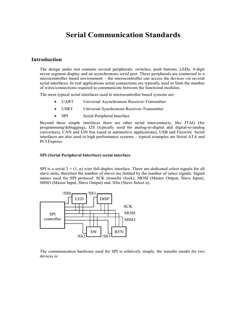
Serial Communication Standards Introduction The design under test contains several peripherals: switches, push buttons, LEDs, 4-digit seven segment display and an asynchronous serial port. These peripherals are connected to a microcontroller based environment – the microcontroller can access the devices via several serial interfaces. In real applications serial connections are typically used to limit the number of wires/connections required to communicate between the functional modules. The most typical serial interfaces used in microcontroller based systems are: UART Universal Asynchronous Receiver-Transmitter USRT Universal Synchronous Receiver-Transmitter SPI Serial Peripheral Interface Beyond these simple interfaces there are other serial interconnects, like JTAG (for programming/debugging), I2S (typically used for analog-to-digital and digital-to-analog converters), CAN and LIN bus (used in automotive applications), USB and Firewire. Serial interfaces are also used in high performance systems – typical examples are Serial ATA and PCI Express. SPI (Serial Peripheral Interface) serial interface SPI is a serial 3 + (1..n) wire full-duplex interface. There are dedicated select signals for all slave units, therefore the number of slaves are limited by the number of select signals. Signal names used for SPI protocol: SCK (transfer clock), MOSI (Master Output, Slave Input), MISO (Master Input, Slave Output) and /SSn (Slave Select n). /SS0 /SS1 LED DISP SCK MOSI SPI controller MISO SW /SS2 BTN /SS3 The communication hardware used for SPI is relatively simple, the transfer model for two devices is: Measurement Laboratory 1., Measurement 3., Serial protocols SPI Master-slave connection Both the master and the slave device contain a shift-register which are operated in parallel with the SCK clock. The master shifts in the MISO signal, while the enabled slave shifts in the MOSI signal. Depending on the clock edge used for the shifting there are 4 different SPI modes: SPI Mode SCK starting edge SCK closing edge 0 Sampling data at rising edge Transmit new data at falling edge 1 Transmit new data at rising edge Sampling data at falling edge 2 Sampling data at falling edge Transmit new data at rising edge 3 Transmit new data at falling edge Sampling data at rising edge Typical waveforms for these modes are shown below. SPI transfer waveforms 2 The following schematic diagram shows a single SPI controller with 4 SPI memories (EEPROM) connected to it. The read timing diagram for an EEPROM is the following: Reading a single byte requires 24 SPI clock cycles. At the beginning of the transfer the SPI chip select signal (CS) goes to low state. In the following 16 clock cycles the controller sends a read instruction and an address on the MOSI wire (SI on the diagram). During this time the EEPROM does not drive its output (the MISO wire, SO on the diagram). During the last 8 clock cycles the EEPROM transmits the data which was read in a serial form, starting with the most significant bit. The write diagram is almost the same. The only difference is that the EEPROM never drives its output, while the SPI controller sends data in all 24 clock cycles: during the first 16 cycles a write command and a write address is sent, while the remaining 8 cycles are used to transmit the data to be written into the EEPROM. 3 Measurement Laboratory 1., Measurement 3., Serial protocols UART serial interface UART is the most widely used serial interface used in embedded systems and desktop environments. The two-wire interface allows full-duplex operation at moderate transfer speeds. Unlike previous protocols, UART is a point-point communication protocol between two devices. One of the wires is driven by one of the devices, while the other is driven by the other device. Both devices have a transmit port (TX) and a receive port (RX). TX RX DEVICE 0 DEVICE 1 RX TX Transferring data is done in characters. A single character may include 5, 6, 7, 8 or 9 data bits, while other bits are used for synchronization and error detection. As UART is asynchronous (no clock signal is transferred between the communicating devices) the transfer bit rate is pre-defined, and can be between 110 bit/sec and 115200 bit/sec. A single data frame is shown below: A single UART frame The transferred bits are: 1 START bit (logic LOW) Various (pre-defined) number of data bits: 5, 6, 7, 8, 9 Optional parity bit (even or odd) 1, 1.5 or 2 STOP bit (logic HIGH) Let us assume that the character “M” is sent in 8E1 mode (8 data bits, even parity, 1 stop bit). The ASCII code of “M” is decimal 77, which is 8’b0100_1101 in binary format. Therefore the waveform of the transmission is the following. IDLE 0 START 1 (LSB) 0 1 1 0 0 1 0 (MSB) 0 1 PAR. STOP IDLE To safely identify the transferred bits, the receiver normally operates at 16x the frequency of the transfer bit rate – that is the receiver takes 16 samples from every incoming bit. The falling edge of the START bit is used as the synchronization point: the 16x sampling start at this point, as shown below. 4 Detecting UART START bit The receiver continuously inspects the incoming signal; after detecting a falling edge it starts to sample the input with the 16x bit-rate. The actual value of a transferred bit is normally determined by samples 8-10 (the middle of an incoming bit). If the first detected value after a falling edge is zero, a START bit was identified. Following bits are sampled/handled according to the pre-defined parameters (number of data bits, parity, number of stop bits). These bits are also sampled at 16x frequency, as shown below: Sampling data bits Data and parity bits are followed by the STOP bit. After receiving this bit, the receiver can immediately accept a new character by monitoring the input line and waiting for a new start bit. It must be noted that the communication is asynchronous, therefore both the transmitter and the receiver generates the communication frequency (baud rate) from its own clock source. This implies that the generated frequencies may differ. For correct communication, sampling positions 8-10 should fall into the time of the last transmitted bit (STOP bit) – otherwise the receiver cannot detect the STOP bit and generates an error. Using this requirement and the number of transmitted bits you can compute the maximum allowed difference between the communication speed of the receiver and transmitter (do this computation!). USRT serial interface USRT is basically the synchronous version of UART: beyond the RX and TX data lines an USRT clock is also present. The frequency of the USRT clock equals to the frequency of the baud rate – therefore it is not necessary for the receiver to generate the baud rate (or 16x baud rate), the USRT clock can be used for sampling the received data or generating the transmitted data. USRT_CLK USRT_RX USRT_TX IDLE 0 START 1 (LSB) 0 1 1 0 0 1 0 (MSB) 0 1 PAR. STOP IDLE For the FPGA in the laboratory, the USRT clock is an incoming signal. However, keep in mind that it is a requirement to use the 50 MHz system clock for all FFs – therefore the 5 Measurement Laboratory 1., Measurement 3., Serial protocols USRT clock cannot be directly connected to the FFs’ clock input. Instead, the rising edge of this clock should be detected and used as an enable signal. 6


