Preliminary data sheet
SKY65142: 100–1000 MHz
Ultra Wideband Variable Gain Amplifier
Applications
Block Diagram
AMPS/PCS/DCS/GSM/EDGE/GPRS
• VHF/UHF TV/Tetra
• Base stations
• Repeaters
VATT
l
VCNT
Features
W
ideband frequency operation: 100–1000 MHz
• Gain control range: 20 dB
• Gain at zero attenuation: 22 dB
• Linear output power > 27 dBm
• Output IP3 > 35 dBm
• Single DC supply: 5 V
• Internal PA RF match with DC block
• Low power consumption, PAE > 35%
• MCM (12-pin 8 x 8 mm) lead (Pb)-free package
(MSL-3, 260 °C per JEDEC J-STD-020)
l
RF Out
Bias Circuit
BIAS
VREF
VCC
NEW
VCNT
GND
Package Diagram
12
11
10
1
9
GND
RFIN
2
8
RFOUT
GND
3
7
GND
4
5
6
VCC
GND
VREF
The VGA maintains very linear performance over a wide frequency bandwidth of 100 MHz to 1 GHz with a P1 dB greater than
27 dBm, OIP3 greater than 35 dBm and gain at zero attenuation
greater than 20 dB.
All active circuitry in the module is contained in a single
Microwave Monolithic Integrated Circuit (MMIC). The device is
fabricated using Skyworks high reliability Aluminum (Al) Gallium
Arsenide (GaAs) Heterojunction Bipolar Transistor (HBT) process,
which allows for single supply operation while maintaining high
efficiency and good linearity.
Output
Match
VATT
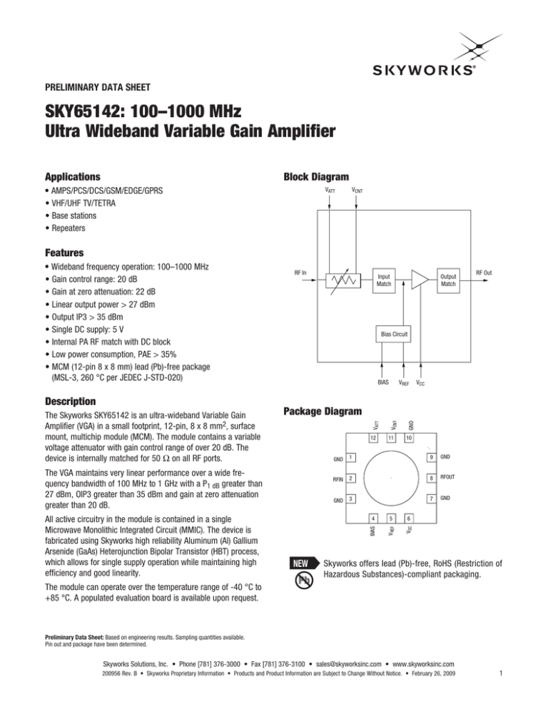
The Skyworks SKY65142 is an ultra-wideband Variable Gain
Amplifier (VGA) in a small footprint, 12-pin, 8 x 8 mm2, surface
mount, multichip module (MCM). The module contains a variable
voltage attenuator with gain control range of over 20 dB. The
device is internally matched for 50 W on all RF ports.
Input
Match
BIAS
Description
RF In
Skyworks offers lead (Pb)-free, RoHS (Restriction of
Hazardous Substances)-compliant packaging.
The module can operate over the temperature range of -40 °C to
+85 °C. A populated evaluation board is available upon request.
Preliminary Data Sheet: Based on engineering results. Sampling quantities available.
Pin out and package have been determined.
Skyworks Solutions, Inc. • Phone [781] 376-3000 • Fax [781] 376-3100 • sales@skyworksinc.com • www.skyworksinc.com
200956 Rev. B • Skyworks Proprietary Information • Products and Product Information are Subject to Change Without Notice. • February 26, 2009
1
preliminary Data Sheet • SKY65142
Operating Characteristics
VCC = VREF = VATT = BIAS = 5 V, VCNT = 0 V, TC = 25 °C, Z0 = 50 W, unless otherwise noted
Parameter
Symbol
Frequency
Condition
Min.
Typ.
F
Max.
Units
156
MHz
Gain at minimum attenuation
Gmax
CW PIN = -15 dBm
22
24
Gain control range
Grange
CW
20
23
dB
Output power at 1 dB compression
P1 dB
CW
27
28.5
dBm
PAE at output P1 dB
PAE
CW
38
44
%
Output 3rd order intercept point
OIP3
POUT/tone = 5 dBm, DF = 1 MHz
32
36
dBm
330
mA
Current at output P1 dB
ICC
Parameter
CW
Symbol
Frequency
Condition
Min.
26
Typ.
F
dB
Max.
Units
450
MHz
Gain at minimum attenuation
Gmax
CW PIN = -15 dBm
20
22
Gain control range
Grange
CW
18
20
dB
Output power at 1 dB compression
P1 dB
CW
26
27.5
dBm
PAE at output P1 dB
PAE
CW
32
38
%
Output 3rd order intercept point
OIP3
POUT/tone = 5 dBm, DF = 1 MHz
32
36.5
dBm
290
mA
Current at output P1 dB
ICC
Parameter
CW
Symbol
Frequency
Condition
Min.
24
Typ.
F
dB
Max.
Units
905
Gain at minimum attenuation
Gmax
CW PIN = -15 dBm
Gain control range
Grange
Output power at 1 dB compression
MHz
18.5
20.5
22.5
dB
CW
18
20
dB
P1 dB
CW
25
26.5
dBm
PAE at output P1 dB
PAE
CW
37
43
%
Output 3rd order intercept point
OIP3
POUT/tone = 5 dBm, DF = 1 MHz
32
36.5
dBm
Current at output P1 dB
ICC
CW
240
v
Quiescent current
ICCQ
No RF
120
mA
Recommended Operating Conditions
Parameter
Supply voltage
2
Symbol
Min.
Typ.
Max.
Unit
VCC, BIAS, VREF, VATT
4.75
5
5.25
V
5
V
Control voltage (maximum atten.)
VCNT
Control voltage (minimum atten.)
VCNT
0
Operating frequency
Fo
100
Operating case temperature
TC
-40
V
+25
1000
MHz
+85
˚C
Skyworks Solutions, Inc. • Phone [781] 376-3000 • Fax [781] 376-3100 • sales@skyworksinc.com • www.skyworksinc.com
February 26, 2009 • Skyworks Proprietary Information • Products and Product Information are Subject to Change Without Notice. • 200956 Rev. B
preliminary Data Sheet • SKY65142
Absolute Maximum Ratings
Characteristic
Value
RF output power
29 dBm
Supply voltage (VCC, BIAS, VREF, VATT)
5.5 V
Supply current (ICC)
1300 mA
Power dissipation (Pdiss)
2W
Operating case temperature (TC)
-40 °C to +85 °C
Storage temperature (TST)
-55 °C to +125 °C
Junction temperature (TJ)
150 °C
Performance is guaranteed only under the conditions listed in the specifications table and is
not guaranteed under the full range(s) described by the Absolute Maximum specifications.
Exceeding any of the absolute maximum/minimum specifications may result in permanent
damage to the device and will void the warranty. Each absolute maximum rating listed is an
individual parameter. Biasing and driving the amplifier with more than one absolute maximum
rating listed may result in permanent damage to the device. Exposure to maximum rating
conditions for extended periods may reduce device reliability.
CAUTION: A lthough this device is designed to be as robust as
possible, Electrostatic Discharge (ESD) can damage
this device. This device must be protected at all
times from ESD. Static charges may easily produce
potentials of several kilovolts on the human body
or equipment, which can discharge without detection. Industry-standard ESD precautions should be
employed at all times.
Typical Performance Data
VCC = VREF = VATT = BIAS = 5 V, VCNT = 0 V, TC = 25 °C, Z0 = 50 W, unless otherwise noted
lS11l
30
lS21l
lS22l
Current (A)
Sij (dB)
905 MHz
0.35
10
450 MHz
0.40
20
0
-10
0.30
0.25
0.20
-20
0.15
-30
0.10
-40
156 MHz
0.45
0
200
400
600
800
1000
1200
0.05
-20
-15
-10
-5
0
5
10
15
Frequency (GHz)
Power In (dBm)
s-Parameters vs. Frequency
Current vs. Power in across Frequency
Skyworks Solutions, Inc. • Phone [781] 376-3000 • Fax [781] 376-3100 • sales@skyworksinc.com • www.skyworksinc.com
200956 Rev. B • Skyworks Proprietary Information • Products and Product Information are Subject to Change Without Notice. • February 26, 2009
3
preliminary Data Sheet • SKY65142
Typical Performance Data
VCC = VREF = VATT = BIAS = 5 V, VCNT = 0 V, TC = 25 °C, Z0 = 50 W, unless otherwise noted
156 MHz
30
450 MHz
815 MHz
905 MHz
25
25
1V
1.5 V
1.75 V
2V
2.5 V
2.75 V
3V
3.2 V
3.5 V
3.75 V
4V
20
15
15
10
Gain (dB)
Gain (dB)
20
0.75 V
2.25 V
5
5
0
-5
10
0.5
1.0
1.5
2.0
2.5
3.0
3.5
0
4.0
-5
VCNT (V)
0
Gain vs. VCnt across Frequency
100 200 300 400 500 600 700 800 900 1000
Frequency (MHz)
32
60
31
55
30
50
29
45
PAE (%)
P1 dB (dBm)
Gain vs. Frequency across VCnt
28
27
30
25
25
20
100 200 300 400 500 600 700 800 900 1000
100 200 300 400 500 600 700 800 900 1000
Frequency (MHz)
Frequency (MHz)
P1 dB vs. Frequency
Pae at P1 dB vs. Frequency
156 MHz
45
450 MHz
815 MHz
905 MHz
43
0
41
-10
39
35
33
31
29
27
25
2nd_VSWR 1:1
2nd_VSWR 5:1
3rd_VSWR 1:1
3rd_VSWR 5:1
-20
37
Harmonics (dBc)
OIP3 (dBm)
35
26
24
-30
-40
-50
-60
-70
0
2.5
5.0
7.5
10.0 12.5
15.0 17.5
20.0
Attenuation Level (dB)
OiP3 vs. attention level across Frequency
POUt = 5 dBm/tone, DF = 1 mhz
4
40
-80
750 770 790 810 830 850 870 890 910 930 950
Frequency (MHz)
2nd and 3rd harmonics vs. Frequency
across VsWr
Skyworks Solutions, Inc. • Phone [781] 376-3000 • Fax [781] 376-3100 • sales@skyworksinc.com • www.skyworksinc.com
February 26, 2009 • Skyworks Proprietary Information • Products and Product Information are Subject to Change Without Notice. • 200956 Rev. B
preliminary Data Sheet • SKY65142
Theory of Operation
The SKY65142 variable gain amplifier is a module comprised
of voltage variable attenuator with a gain control range of over
20 dB and a single amplifier stage providing 20 dB of gain at
zero attenuation. The device is internally matched for 50 W on
all RF ports. An in module active bias circuit is included within
the device providing for excellent gain tracking over temperature
and voltage variations.
The SKY65142 attenuator consists of 2 parallel, shunt PIN
diodes controlled by an externally supplied bias via VCNT, Pin
11. VCNT operates over a range of 0–5 V with 5 V providing
maximum attenuation. VATT, pin 12, is the bias voltage for the
attenuator circuit.
The SKY65142 amplifier is internally matched for optimum
linearity and efficiency. It is independently supplied using the VCC
supply line, pin 6. The bias reference voltage is supplied using the
VREF line, pin 5. The DC control voltage that sets the bias to the
amplifier is supplied via the BIAS line, pin 4.
Application Circuit Notes
Center Ground. It is extremely important that the device paddle
be sufficiently grounded for both thermal and stability reasons.
Multiple small vias are acceptable and will work well under the
device if solder migration is an issue.
Ground (Pins 1, 3, 7, 9, 10). Attach all ground pins to the RF
ground plane with the largest diameter and lowest inductance
via that the layout will allow. Multiple small vias are also acceptable and will work well under the device if solder migration is an
issue.
VCNT (Pin 11). VCNT is the amplifier gain control voltage. Nominal
operating range is between 0–5 V, with 5 V with 5 V providing
maximum attenuation.
VATT (Pin 12). VATT is the bias voltage for the attenuator
circuit (typically 5 V). DC bypass is provided by capacitor C7.
Package and Handling Information
Since the device package is sensitive to moisture absorption, it
is baked and vacuum packed before shipping. Instructions on the
shipping container label regarding exposure to moisture after the
container seal is broken must be followed. Otherwise, problems
related to moisture absorption may occur when the part is subjected to high temperature during solder assembly.
Please refer to Skyworks solder reflow application note, available at www.skyworksinc.com, for instructions on mounting the
SKY65142 to a printed circuit board.
Production quantities of this product are shipped in a standard tape and reel format. For packaging details, refer to the
Skyworks Application Note, Tape and Reel, document number
101568.
Electrostatic Discharge (ESD) Sensitivity
The SKY65142 is a static-sensitive electronic device. Do not
operate or store near strong electrostatic fields. Take proper ESD
precautions.
RFIN (Pin 2). Module RF Input Pin. ZO = 50 W. The module
includes an onboard internal DC blocking capacitor. All impedance matching is provided internal to the module.
BIAS (Pin 4). BIAS is the bias supply voltage for the amplifier,
typically set to 5 V. Bypass capacitors C11and C14 have been
utilized to ensure stability both in and out of the useable bandwidth of the device.
VREF (Pin 5). Bias reference voltage for the amplifier. VREF should
be operated over the same voltage range as VCC, with a nominal
voltage of 5 V. Resistor, R1 sets the optimal voltage at the
package pin.
VCC (Pin 6). Supply voltage for the amplifier collector bias (typically 5 V). Bypassing of VCC is accomplished with inductor L1
and capacitors C9, C10 and C15. They should be placed in the
approximate location shown on the evaluation board, but placement is not critical.
RFOUT (Pin 8). Module RF Output Pin. ZO = 50 W. The module
includes an onboard internal DC blocking capacitor. All impedance matching is provided internal to the module.
Skyworks Solutions, Inc. • Phone [781] 376-3000 • Fax [781] 376-3100 • sales@skyworksinc.com • www.skyworksinc.com
200956 Rev. B • Skyworks Proprietary Information • Products and Product Information are Subject to Change Without Notice. • February 26, 2009
5
preliminary Data Sheet • SKY65142
Pin Assignments
Evaluation Board Test Procedure
Pin #
Name
1
GND
Ground
2
RFIN
RF input
3
GND
Ground
4
BIAS
Amplifier bias voltage
5
VREF
Amplifer reference voltage
6
VCC
Amplifer supply voltage
7
GND
Ground
8
RFOUT
9
GND
Ground
10
GND
Ground
11
VCNT
Amplifier gain control voltage
12
VATT
Attenuator bias voltage
Use the following procedure to set up the SKY65142 evaluation
board for testing.
Description
1. Connect 5 V DC supply voltages to BIAS, and VREF. If available,
enable the current limiting function of these power supplies
to 0.1 A.
2. Connect a 5 V to the attenuators supply voltages, VATT and
VCNT. If available, enable the current limiting function of the
power supply to 0.05 A.
3. Connect a 5 V to the amplifier supply voltage, VCC. If available,
enable the current limiting function of the power supply to 1.3 A.
RF output
4. Connect signal generator(s) to the required RF input port.
Set the desired RF signal frequency. Set RF power level to
8 dBm or less to the evaluation board but do NOT enable the
RF signal.
Center attachment pad must have a low inductance and low thermal resistance connection to
the customer’s printed circuit board ground plane.
6. Enable the RF signal.
Application Circuit
VATT
C7
1500 pF
VCNT
7. Take measurements.
C12
DNI
CAUTION: If the input signal exceeds the rated power, the
SKY65142 Evaluation Board can be permanently
damaged.
2
RFIN
10
11
GND
VCNT
GND
VATT 12
J8
1
SKY65142
NOTE: It is important that the VCC voltage source be adjusted
such that 5.0 V is measured at the board. The high
collector currents will drop the collector voltage
significantly if long leads are used. Adjust the bias
voltage to compensate.
9
8
RFOUT
SMA
SMA
GND
7
GND
VCC
Refer to the “Recommended Solder Reflow Profile”
Application Note.
L1
68 nH
C9
150 pF
C8
DNI
C10
0.01 µF
R1
150 Ω
C11
0.01 µF
C14
10 µF
BIAS
Recommended Solder Reflow Profiles
6
5
4
VREF
BIAS
3
6
5. Set the desired attenuation by adjusting the voltage level on
VCNT supply lines. (0 V = minimum attenuation,
5 V = maximum attenuation).
C13
1000 pF
VREF
Tape and Reel Information
Refer to the “Discrete Devices and IC Switch/Attenuators
Tape and Reel Package Orientation” Application Note.
C15
10 µF
VCC
Skyworks Solutions, Inc. • Phone [781] 376-3000 • Fax [781] 376-3100 • sales@skyworksinc.com • www.skyworksinc.com
February 26, 2009 • Skyworks Proprietary Information • Products and Product Information are Subject to Change Without Notice. • 200956 Rev. B
preliminary Data Sheet • SKY65142
Evaluation Board
Evaluation Board Description
VATT
VCNT
GND
GND
The Skyworks SKY65142 evaluation board is used to test the
performance of the SKY65142 power amplifier module. The
following design considerations are general in nature and must
be followed regardless of final use or configuration.
1. Paths to ground should be made as short as possible.
RF Out
BIAS
VREF
VCC
GND
RF In
2. The ground pad of the SKY65142 power amplifier module has
special electrical and thermal grounding requirements. This
pad is the main thermal conduit for heat dissipation. Since
the circuit board acts as the heat sink, it must shunt as much
heat as possible from the amplifiers. As such, design the connection to the ground pad to dissipate the maximum wattage
produced to the circuit. Multiple vias to the grounding layer are
required.
3. Bypass capacitors should be used on the DC supply lines. RF
inductor is required on the VCC supply line to block RF signal
from the DC supply. See evaluation board schematic drawing
for more details.
4. The RF lines should be well separated from each other, with
solid ground in between traces, to maximize input-to-output
isolation.
NOTE: Junction temperature (TJ) of the device increases with a
poor connection to the slug and ground. This reduces the
lifetime of the device.
Evaluation Board Layer Detail
Layer 1: Silk Screen
Layer 1: Top Metal
Layer 2 and 3: Ground
Layer 4: Ground
Skyworks Solutions, Inc. • Phone [781] 376-3000 • Fax [781] 376-3100 • sales@skyworksinc.com • www.skyworksinc.com
200956 Rev. B • Skyworks Proprietary Information • Products and Product Information are Subject to Change Without Notice. • February 26, 2009
7
preliminary Data Sheet • SKY65142
Bill of Material for Evaluation Board
Part
ID
Qty.
Size
Value
Units
Product Number
Manufacturer
Manufacturer’s Part Number
Characteristics
1
C7
1
0603
1500
pF
SK204-000-003
Murata
GRM1885C1H152JA01D
C0G, 50 V, ± 5%
2
C9
1
0603
150
pF
SK204-000-020
Murata
GRM1885C1H151JA01D
C0G, 50 V, ± 5%
3
C10, C11
2
0603
0.01
µF
SK204-000-013
Murata
GCM188R71H103KA37D
X7R, 50 V, ± 5%
4
C13
1
0805
1000
pF
5404R19-037
Murata
GRM2195C1H102JDX1D
C0G, 50 V, ± 5%
5
C14, C15
2
1206
10
µF
Matsuo
267M1602106K-720
Tantalum, 16 V, ± 10%
6
L1
1
0805
68
nH
CoilCraft
0805CS-680XJLB
5%, SRF 1500 MHz
7
R1
1
0603
150
W
Rohm
MCR03EZHUJ150
50 V, 0.063 W, ± 5%
8
C8, C12
5424R36-029
Do Not Install
Evaluation Board Stack-Up
Cross Section
Branding Specifications
Type
Thick
Material
εr
Pri
Electrical
0.035 mm
Cu
0.0
Die 1
Isolation
0.3 mm
RO4003-12-3.38
3.38
L2
Die 2
L3
Plane
Isolation
Plane
0.035 mm
0.1 mm
0.035 mm
CU
FR4
CU
0.0
4.0
0.0
Die 3
Isolation
0.3 mm
FR4
4.0
Sec
Electrical
0.035 mm
CU
0.0
Name
Mark Pin 1
Identifier
Manufacturing Part Number
Revision Number
SKY65142-21
EXXXXX.XX
YYWW MX
Lot Number
YY = Manufacture Year
WW = Week Packaged
Sealed
MX = Country Code
Tape and Reel Dimensions
Pin #1
indicator
12.00 ± 0.02
2.00 ± 0.05
4.00
1.55 ± 0.05
5o
A
1.75 ± 0.10
7.50 ± 0.05
B
A
16.00 ± 0.03
0.30 ± 0.05
8.35
1.50 Min.
B
1.70
5o
B
Notes:
1. Carrier tape material: black conductive polystyrene
2. Cover tape material: transparent conductive PSA
3. Cover tape size: 13.3 mm width
4. All measurements are in millimeters
8
8.35
A
Skyworks Solutions, Inc. • Phone [781] 376-3000 • Fax [781] 376-3100 • sales@skyworksinc.com • www.skyworksinc.com
February 26, 2009 • Skyworks Proprietary Information • Products and Product Information are Subject to Change Without Notice. • 200956 Rev. B
preliminary Data Sheet • SKY65142
Package Outline and Recommended Footprint
8.685 mm
12X 0.81 mm
12X 1.043 mm
8.385
Pin 1 Indicator
2X 1.65 mm
Top
8.385
2X 1.91mm
8.685 mm
6X 4.093
1.45 ± 0.1
Stencil Aperture Size of 60 to
80% of the Module/Pkg
Solder Mask Area
(Ø0.3)
Solder Mask Opening
(Ø0.15) Metal Pad
Pin 1 Indicator
(3.4)
Pin 12
Pin 1
0
0
4X 1.65
6X 4.093
5.080 Solder
Mask Opening
0.793 ± 0.1
(0.1)
Metal Pad Edge
6X 0.81 mm
1.65 mm Typ.
6X 1.043 mm
8.685 mm
Package Outline
Stencil Aperture
Top View
(2.7)
A
4X 1.91
Package Outline
8.685 mm
Pin 12
Package Outline
12X SMT Pad
CL
Pin 1
CL
1.91 mm Typ.
0.25 mm
Thermal Via Array
Ø0.3 mm On 0.6 mm Pitch
Additional Vias in Common Ground Pad
Will Improve Thermal Performance
CL
Metallization
Top View
0.81 ± 0.05
Detail A
8.785 mm
1.65 mm
Pin 12
12X 1.143 mm
Pin 1
12X 0.91 mm
CL
Package Outline
1.91mm Typ.
8.785 mm
CL
5.080
Solder Mask
Opening
Solder Mask Opening
Top View
Skyworks Solutions, Inc. • Phone [781] 376-3000 • Fax [781] 376-3100 • sales@skyworksinc.com • www.skyworksinc.com
200956 Rev. B • Skyworks Proprietary Information • Products and Product Information are Subject to Change Without Notice. • February 26, 2009
9
preliminary Data Sheet • SKY65142
Ordering Information
Model Name
SKY65142: 100-1000 MHz Ultra Wideband Variable Gain Amplifier
Manufacturing Part Number
Evaluation Kit Part Number
SKY65142-21 (Pb-free package)
TW13-D965-009
Copyright © 2008, Skyworks Solutions, Inc. All Rights Reserved.
Information in this document is provided in connection with Skyworks Solutions, Inc. (“Skyworks”) products or services. These materials, including the information contained herein, are provided
by Skyworks as a service to its customers and may be used for informational purposes only by the customer. Skyworks assumes no responsibility for errors or omissions in these materials or the
information contained herein. Skyworks may change its documentation, products, services, specifications or product descriptions at any time, without notice. Skyworks makes no commitment to
update the materials or information and shall have no responsibility whatsoever for conflicts, incompatibilities, or other difficulties arising from any future changes.
No license, whether express, implied, by estoppel or otherwise, is granted to any intellectual property rights by this document. Skyworks assumes no liability for any materials, products or
information provided hereunder, including the sale, distribution, reproduction or use of Skyworks products, information or materials, except as may be provided in Skyworks Terms and
Conditions of Sale.
THE MATERIALS, PRODUCTS AND INFORMATION ARE PROVIDED “AS IS” WITHOUT WARRANTY OF ANY KIND, WHETHER EXPRESS, IMPLIED, STATUTORY, OR OTHERWISE, INCLUDING FITNESS FOR A
PARTICULAR PURPOSE OR USE, MERCHANTABILITY, PERFORMANCE, QUALITY OR NON-INFRINGEMENT OF ANY INTELLECTUAL PROPERTY RIGHT; ALL SUCH WARRANTIES ARE HEREBY EXPRESSLY
DISCLAIMED. SKYWORKS DOES NOT WARRANT THE ACCURACY OR COMPLETENESS OF THE INFORMATION, TEXT, GRAPHICS OR OTHER ITEMS CONTAINED WITHIN THESE MATERIALS. SKYWORKS
SHALL NOT BE LIABLE FOR ANY DAMAGES, INCLUDING BUT NOT LIMITED TO ANY SPECIAL, INDIRECT, INCIDENTAL, STATUTORY, OR CONSEQUENTIAL DAMAGES, INCLUDING WITHOUT LIMITATION,
LOST REVENUES OR LOST PROFITS THAT MAY RESULT FROM THE USE OF THE MATERIALS OR INFORMATION, WHETHER OR NOT THE RECIPIENT OF MATERIALS HAS BEEN ADVISED OF THE
POSSIBILITY OF SUCH DAMAGE.
Skyworks products are not intended for use in medical, lifesaving or life-sustaining applications, or other equipment in which the failure of the Skyworks products could lead to personal injury,
death, physical or environmental damage. Skyworks customers using or selling Skyworks products for use in such applications do so at their own risk and agree to fully indemnify Skyworks for any
damages resulting from such improper use or sale.
Customers are responsible for their products and applications using Skyworks products, which may deviate from published specifications as a result of design defects, errors, or operation of
products outside of published parameters or design specifications. Customers should include design and operating safeguards to minimize these and other risks. Skyworks assumes no liability for
applications assistance, customer product design, or damage to any equipment resulting from the use of Skyworks products outside of stated published specifications or parameters.
Skyworks, the Skyworks symbol, and “Breakthrough Simplicity” are trademarks or registered trademarks of Skyworks Solutions, Inc., in the United States and other countries. Third-party brands
and names are for identification purposes only, and are the property of their respective owners. Additional information, including relevant terms and conditions, posted at www.skyworksinc.com, are
incorporated by reference.
10
Skyworks Solutions, Inc. • Phone [781] 376-3000 • Fax [781] 376-3100 • sales@skyworksinc.com • www.skyworksinc.com
February 26, 2009 • Skyworks Proprietary Information • Products and Product Information are Subject to Change Without Notice. • 200956 Rev. B


