TS3005
A 1.55V to 5.25V, 1.35µA, 1.7ms to 33hrs Silicon Timer
FEATURES
DESCRIPTION
The TS3005 is a single-supply, second-generation
oscillator/timer fully specified to operate at a supply
voltage range of 1.55V to 5.25V while consuming less
than 1.5μA(max) supply current. Requiring only a
resistor to set the base output frequency (or output
period) at 49Hz (or 20.5ms) with a 50% duty cycle,
the TS3005 timer/oscillator is compact, easy-to-use,
and versatile. Optimized for ultra-long life, low
frequency, battery-powered/portable applications, the
TS3005 joins the TS3001, TS3002, TS3003, TS3004,
and TS3006 in the CMOS timer family of “NanoWatt
Analog™” high-performance analog integrated
circuits.
Ultra Low Supply Current: 1.35μA at 49Hz
Supply Voltage Operation: 1.55V to 5.25V
Single Resistor Sets FOUT at 50% Duty Cycle
3-pin User-Programmable FOUT Period:
1.7ms ≤ tFOUT ≤ 33hrs
FOUT Period Accuracy: 3%
FOUT Period Drift: 0.02%/ºC
Single Resistor Sets Output Frequency
Separate PWM Control and Buffered Output
FOUT/PWMOUT Output Driver Resistance:
160Ω
APPLICATIONS
Portable and Battery-Powered Equipment
Low-Parts-Count Nanopower Oscillator
Compact Micropower Replacement for Crystal and
Ceramic Oscillators
Micropower Pulse-width Modulation Control
Micropower Pulse-position Modulation Control
Micropower Clock Generation
Micropower Sequential Timing
The TS3005 output period can be user-adjusted from
1.7ms to 33hrs without additional components. In
addition, the TS3005 represents a 25% reduction in
pcb area and a factor-of-10 lower power consumption
over
other
CMOS-based
integrated
circuit
oscillators/timers. When compared against industrystandard 555-timer-based products, the TS3005
offers up to 84% reduction in pcb area and over three
orders of magnitude lower power consumption.
The TS3005 is fully specified over the -40°C to +85°C
temperature range and is available in a low-profile,
10-pin 3x3mm TDFN package with an exposed
back-side paddle.
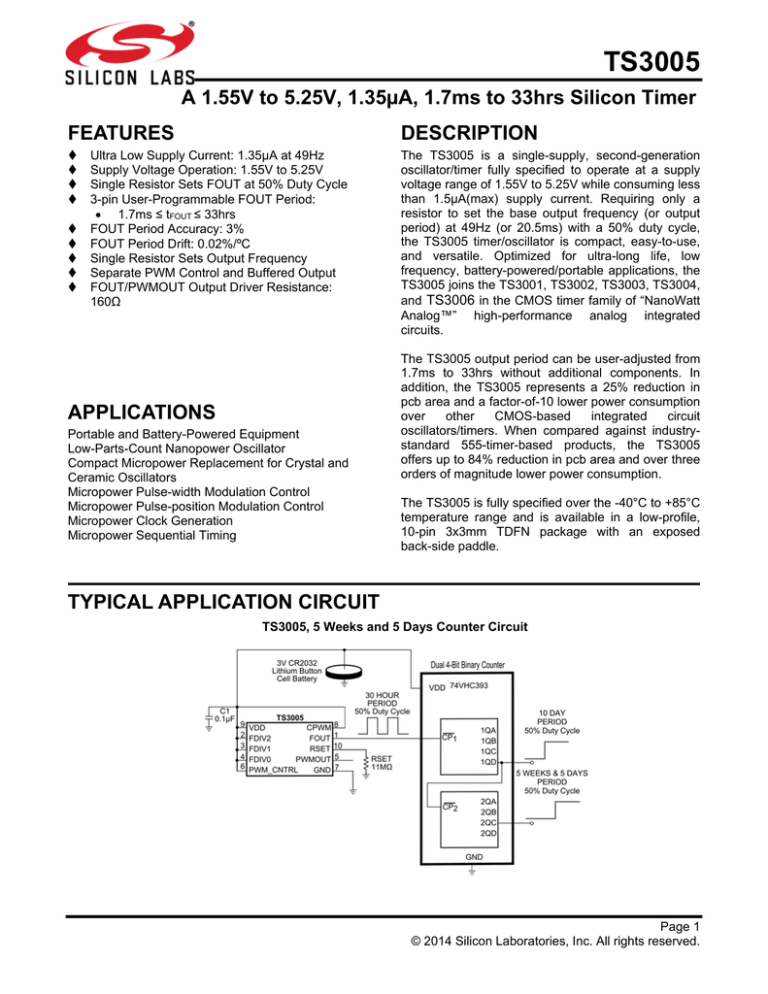
TYPICAL APPLICATION CIRCUIT
TS3005, 5 Weeks and 5 Days Counter Circuit
Page 1
© 2014 Silicon Laboratories, Inc. All rights reserved.
TS3005
ABSOLUTE MAXIMUM RATINGS
VDD to GND................................................................. -0.3V to +5.5V
PWM_CNTRL to GND ................................................ -0.3V to +5.5V
FOUT, PWMOUT to GND .......................................... -0.3V to +5.5V
RSET to GND............................................................. -0.3V to +2.5V
CPWM to GND ........................................................... -0.3V to +5.5V
FDIV to GND .............................................................. -0.3V to +5.5V
Continuous Power Dissipation (TA = +70°C)
10-Pin TDFN (Derate at 13.48mW/°C above +70°C) ... 1078mW
Operating Temperature Range ................................. -40°C to +85°C
Storage Temperature Range .................................. -65°C to +150°C
Lead Temperature (Soldering, 10s)...................................... +300°C
Electrical and thermal stresses beyond those listed under “Absolute Maximum Ratings” may cause permanent damage to the device. These
are stress ratings only and functional operation of the device at these or any other condition beyond those indicated in the operational sections
of the specifications is not implied. Exposure to any absolute maximum rating conditions for extended periods may affect device reliability and
lifetime.
PACKAGE/ORDERING INFORMATION
ORDER NUMBER
PART
CARRIER QUANTITY
MARKING
TS3005ITD1033
Tape
& Reel
-----
Tape
& Reel
3000
3005I
TS3005ITD1033T
Lead-free Program: Silicon Labs supplies only lead-free packaging.
Consult Silicon Labs for products specified with wider operating temperature ranges.
Page 2
TS3005 Rev. 1.0
TS3005
ELECTRICAL CHARACTERISTICS
VDD = 3V, VPWM_CNTRL= VDD, RSET = 4.32MΩ, RLOAD(FOUT) = Open Circuit, CLOAD(FOUT) = 0pF, CLOAD(PWM) = 0pF, CPWM = 47pF, FDIV2:0 = 000 unless
otherwise noted. Values are at TA = 25°C unless otherwise noted. See Note 1.
PARAMETER
Supply Voltage
SYMBOL
VDD
CONDITIONS
CPWM = VDD
Supply Current
IDD
MIN
1.55
TYP
1.35
-40°C ≤ TA ≤ 85°C
1.47
-40°C ≤ TA ≤ 85°C
FOUT Period
FOUT Period Line
Regulation
tFOUT
∆tFOUT/V
-40°C ≤ TA ≤ 85°C
1.55V ≤ VDD ≤ 5.25V
49
∆tFOUT/∆T
PWMOUT Duty Cycle
DC(PWMOUT)
PWMOUT Duty Cycle
Line Regulation
ΔDC(PWMOUT)/V
CPWM Sourcing Current
ICPWM
UVLO Hysteresis
FOUT, PWMOUT
Rise Time
FOUT, PWMOUT
Fall Time
VUVLO
FDIV Input Current
51
0.08
0.02
1.55V < VDD < 5.25V, FDIV2:0 = 000
FDIV2:0 = 000, 001
FDIV2:0 000, 001
(VDD=1.55V) – (VDD_SHUTDOWN VOLTAGE)
0.12
0.03
930
810
%
%
%
1050
1150
97
150
ms
%/°C
-3
-40°C ≤ TA ≤ 85°C
µA
%/V
0.02
VPWM_CNTRL= 0V
UNITS
V
250
nA
nA
mV
tRISE
See Note 2, CL = 15pF
10
ns
tFALL
See Note 2, CL = 15pF
10
ns
0.001
%
FOUT Jitter
RSET Pin Voltage
20.5
0.17
FOUT Duty cycle
FOUT Period
Temperature
Coefficient
19.95
19.4
MAX
5.25
1.5
1.9
1.7
2.1
21.05
21.5
See Note 3
V(RSET)
IFDIV
0.3
V
10
nA
-40°C ≤ TA ≤ 85°C
20
Maximum Oscillator
Fosc
RSET= 360K
586
Hz
Frequency
High Level Output
IOH = 1mA
160
mV
Voltage, FOUT and
VDD - VOH
PWMOUT
Low Level Output
Voltage, FOUT and
VOL
IOL = 1mA
140
mV
PWMOUT
Dead Time
TDT
FOUT edge falling and PWMOUT edge rising
106
ns
Note 1: All devices are 100% production tested at TA = +25°C and are guaranteed by characterization for TA = TMIN to TMAX, as specified.
Note 2: Output rise and fall times are measured between the 10% and 90% of the VDD power-supply voltage levels. The specification is based
on lab bench characterization and is not tested in production.
Note 3: Timing jitter is the ratio of the peak-to-peak variation of the period to the mean of the period. The specification is based on lab bench
characterization and is not tested in production.
TS3005 Rev. 1.0
Page 3
TS3005
TYPICAL PERFORMANCE CHARACTERISTICS
VDD = 3V, VPWM_CNTRL= VDD, RSET = 4.32MΩ, RLOAD(FOUT) = Open Circuit, CLOAD(FOUT) = 0pF, CLOAD(PWM) = 0pF, CPWM = VDD, FDIV2:0 = 000
unless otherwise noted. Values are at TA = 25°C unless otherwise noted.
FOUT Period vs Temperature
Supply Current vs FOUT Period
7
21.5
21
5
PERIOD - ms
SUPPLY CURRENT - µA
6
4
3
2
20
1
0
19.5
0
10.4
20.8
31.2
41.6
52
-40
35
60
Supply Current vs CLOAD(FOUT)
Supply Current vs Temperature
85
1.5
SUPPLY CURRENT - µA
SUPPLY CURRENT - µA
10
TEMPERATURE - ºC
4
2
1.4
1.3
1.2
1.1
0
0
10
30
20
40
-40
10
35
60
TEMPERATURE - ºC
FOUT Period vs Supply Voltage
Start-up Time vs Supply Voltage
85
21
START-UP TIME - ms
20.7
20.6
20.5
20.4
20.3
1.55
-15
CLOAD- pF
20.8
20
19
18
17
16
15
2.29
3.03
3.77
4.51
SUPPLY VOLTAGE - Volt
Page 4
-15
PERIOD - ms
6
PERIOD - ms
20.5
5.25
1.55
2.29
3.03
3.77
4.51
5.25
SUPPLY VOLTAGE - Volt
TS3005 Rev. 1.0
TS3005
TYPICAL PERFORMANCE CHARACTERISTICS
VDD = 3V, VPWM_CNTRL= VDD, RSET = 4.32MΩ, RLOAD(FOUT) = Open Circuit, CLOAD(FOUT) = 0pF, CLOAD(PWM) = 0pF, CPWM = VDD, FDIV2:0 = 000
unless otherwise noted. Values are at TA = 25°C unless otherwise noted.
Supply Current Distribution
60
35%
50
30%
PERCENT OF UNITS - %
PERIOD - ms
Period vs RSET
40
30
20
10
25%
20%
15%
10%
5%
0%
0
0
2
4
6
8
10
12
1.26
RSET - MΩ
1.3
1.34
1.38
SUPPLY CURRENT - µA
FOUT
VDD = 5V, CLOAD = 15pF
FOUT
1V/DIV
FOUT
1V/DIV
FOUT
VDD = 3V, CLOAD = 15pF
FOUT and PWMOUT
VDD = 3V, CLOAD = 15pF, VPWM CNTRL= VDD, CPWM = 10nF
FOUT and PWMOUT
VDD = 5V, CLOAD = 15pF, VPWM CNTRL= VDD, CPWM = 10nF
PWMOUT
2V/DIV
PWMOUT
2V/DIV
FOUT
2V/DIV
5ms/DIV
FOUT
2V/DIV
5ms/DIV
5ms/DIV
TS3005 Rev. 1.0
5ms/DIV
Page 5
TS3005
PIN FUNCTIONS
Page 6
PIN
NAME
1
FOUT
2,3,4
FDIV2:0
5
PWMOUT
6
PWM_CNTRL
7
GND
8
CPWM
9
VDD
10
RSET
FUNCTION
Fixed Frequency Output. A push-pull output stage with an
output resistance of 160Ω. FOUT pin swings from GND to
VDD. For lowest power operation, capacitance loads should
be minimized and resistive loads should be maximized.
Frequency Divider Input. Various combinations of these
inputs will change the FOUT frequency for a fixed value of
RSET. Refer to Table 1.
Pulse-width Modulated Output. A push-pull output stage with
an output resistance of 160Ω, the PWMOUT pin is wired
anti-phase with respect to FOUT and swings from GND to
VDD. For lowest power operation, capacitance loads should
be minimized and resistive loads should be maximized.
PWM Output Pulse Control Pin. Applying a voltage between
GND and VRSET will reduce the duty cycle of the PWMOUT
output that is set by the capacitor connected to the CPWM
pin. Connect PWM_CNTRL to VDD for fixed PWMOUT
output pulse time (determined only by capacitor at CPWM).
Ground. Connect this pin to the system’s analog ground
plane.
PWMOUT Pulse Width Programming Capacitance Input. A
target capacitance connected from this pin to GND sets the
duty cycle of the PMW output. Minimize any stray
capacitance on this pin. The voltage on this pin will swing
from GND to VRSET. Connect CPWM to VDD to disable PWM
function (saves PWM current).
Power Supply Voltage Input. The supply voltage range is
1.55V ≤ VDD ≤ 5.25V. Bypass this pin with a 0.1uF ceramic
coupling capacitor in close proximity to the TS3005.
FOUT Programming Resistor Input. A 4.32MOhm resistor
connected from this pin to ground sets the T3005’s internal
oscillator’s output period to 20ms (49Hz). For optimal
performance, the composition of the RSET resistor shall be
consistent with a tolerance of 1% or lower. The RSET pin
voltage is approximately 0.3V.
TS3005 Rev. 1.0
TS3005
BLOCK DIAGRAM
ICPWM
FDIV
FOUT (Hz)
tFOUT(s)
(A)
2:0
000
1.7ms-56.88ms
586-17.578
1µ
001
13.65ms-455.16ms
73.25-2.197
1µ
010
109.17ms-3.64
9.16-0.2746
100n
011
877.19ms-29.15
1.14-0.0343
100n
100
7.01-233.1
0.143-0.00429
100n
101
55.94-31.09min
0.0178-0.536mHz
100n
110
7.49min-4.146hrs
0.0022-0.0670mHz
100n
111
59.67min-33.1hrs
0.279mHz-8.381µHz
100n
Table 1: FOUT and PWMOUT Frequency Range per FDIV2:0 Combination
TS3005 Rev. 1.0
Page 7
TS3005
THEORY OF OPERATION
The TS3005 is a user-programmable oscillator where
the period of the square wave at its FOUT terminal is
generated by an external resistor connected to the
RSET pin. The output period is given by:
tFOUT (s) =
8FDIV2:0 x RSET x 512
1.08E11
Equation 1. FOUT Frequency Calculation where
FDIV2:0 = 0 to 7
With an RSET = 4.32MΩ and FDIV2:0=111, the FOUT
period is approximately 715.88 minutes with a 50%
duty cycle. As design aids, Tables 2 lists TS3004’s
typical FOUT period for various standard values for
RSET and FDIV2:0 = 111(7).
The output period can be user-adjusted from 1.7ms
to 33hrs without additional components. Frequency
divider inputs FDIV2:0 can be set to a logic state
HIGH or LOW in order to set the desired frequency
as shown in to Table 1.
The TS3005 also provides a separate PWM output
signal at its PWMOUT terminal that is anti-phase with
respect to FOUT. A dead time of approximately
106ns exists between FOUT and PWMOUT. To
adjust the pulse width of the PWMOUT output, a
single capacitor can be placed at the CPWM pin. To
determine the capacitance needed for a desired
pulse width, the following equation is to be used:
Pulse Width(s) x ICPWM
CPWM(F)=
VCPWM ≅300mV
Equation 2. CPWM Capacitor Calculation
where ICPWM and VCPWM is the current supplied and
voltage applied to the CPWM capacitor, respectively.
The pulse width is determined based on the period of
FOUT and should never be greater than the period at
FOUT. Make sure the PWM_CNTRL pin is set to at
least 400mV when calculating the pulse width of
PWMOUT. Note VCPWM is approximately 300mV,
which is the RSET voltage. Also note that ICPWM is
either 1µA or 100nA. Refer to Table 1.
The PWMOUT output pulse width can be adjusted
further after selecting a CPWM capacitor This can be
achieved by applying a voltage to the PWM_CNTRL
pin between VRSET and GND. With a voltage of at
least VRSET, the pulse width is set based on Equation
2. For example, with a period of 20.5ms( 49Hz) a
10nF capacitor at the CPWM pin generates a pulse
width of approximately 3ms. This can be calculated
RSET (MΩ)
tFOUT
0.360
59.67min
1
1.09hrs
2.49
6.87hrs
4.32
11.93hrs
6.81
18.81hrs
9.76
26.93hrs
12
33.1hrs
Table 2: tFOUT vs RSET for FDIV2:0 = 111(7)
using equation 2. By reducing the PWM_CNTRL
voltage from VRSET ≅ 300mV to GND, the pulse width
can be reduced further. Note that as the FOUT
frequency increases, the amount of pulse width
reduction reduces and vice versa. Furthermore, if the
PWMOUT output is half the frequency of the FOUT
output, this means your CPWM capacitor is too large
and as a result, the pulse width is greater than the
FOUT period. In this case, use Equation 2 and
reduce the capacitor value to less than the period.
Connect CPWM to VDD to disable the PWM function
and in turn, save power. Connect PWM_CNTRL to
VDD for a fixed PWMOUT output pulse width, which
is determined by the CPWM pin capacitor only.
APPLICATIONS INFORMATION
Minimizing Power Consumption
To keep the TS3005’s power consumption low,
resistive loads at the FOUT and PWMOUT terminals
increase dc power consumption and therefore should
be as large as possible. Capacitive loads at the
FOUT and PWMOUT terminals increase the
TS3005’s transient power consumption and, as well,
should be as small as possible.
One challenge to minimizing the TS3005’s transient
power consumption is the probe capacitance of
oscilloscopes and frequency counter instruments.
Most instruments exhibit an input capacitance of
15pF or more. Unless buffered, the increase in
transient load current can be as much as 400nA.
To minimize capacitive loading, the technique shown
CEXT =
1
1
1
-
CLOAD(EFF) CPROBE
Equation 3:External Capacitor Calculation
Figure 1: Using an External Capacitor in Series with
Probes Reduces Effective Capacitive Load.
Page 8
TS3005 Rev. 1.0
TS3005
in Figure 1 can be used. In this circuit, the principle of
series-connected capacitors can be used to reduce
the effective capacitive load at the TS3005’s FOUT
and PWMOUT terminals.
For example, if the instrument’s input probe
capacitance is 15pF and the desired effective load
capacitance at either or both FOUT and PWMOUT
To determine the optimal value for CEXT once the
probe capacitance is known by simply solving for
using
the
following
expression:
CEXT
TS3005 Start-up Time
As the TS3005 is powered up, its FOUT terminal
(and PWMOUT terminal, if enabled) is active once
Figure 2: 5 Weeks and 5 Days Counter Circuit
terminals is to be ≤5pF, then the value of CEXT should
be ≤7.5pF.
the applied VDD is higher than 1.55V. Once the
applied VDD is higher than 1.55V, the master
oscillator achieves steady-state operation within
18ms.
5 Weeks and 5 Days Counter Circuit with TS3005
The TS3005 can be configured into a 5 Weeks and 5
Days counter as shown in Figure 2. The circuit is
composed of a TS3005 timer and a dual 74VHC393
4-bit counter. The TS3005 divider inputs are set to
FDIV2:0 = 111. With an RSET of 11MΩ, the FOUT
period is approximately 30 hours. The complete
circuit consumes approximately 4.5µA and is
powered with a single 3V CR2032 lithium button cell
battery. If a shorter period is desired, a 10 day period
is available via output 1QD.
TS3005 Rev. 1.0
Divide the PWMOUT Output Frequency by Two
with the TS3005
Using a single resistor and capacitor, the TS3005 can
be configured to a divide by two circuit as shown in
Figure 3. To achieve a divide by two function with the
TS3005, the pulse width of the PWMOUT output
must be at least a factor of 2 greater than the period
set at FOUT by resistor RSET. The CPWM capacitor
selected must meet this pulse width requirement and
Figure 3: Configuring the TS3005 into a Divide by
Two Frequency Divider
Page 9
TS3005
Using the TS3005 and a Potentiometer to Dim an
LED
Figure 4: Flashing Railroad Lights with the TS3005
can be calculated using Equation 2. In Figure 3, a
value of 4.32MΩ for RSET sets the FOUT output
period to 20.5ms. A CPWM capacitor of 0.1µF was
chosen, which sets the pulse width of PWMOUT to
approximately 30ms. This is well above the required
minimum pulse width of 20.5ms.
The TS3005 can be configured to dim an LED by
modulating the pulse width of the PWMOUT output.
With the input divider set to FDIV2:0 = 000 and
RSET= 2MΩ, the FOUT output frequency is
approximately 100Hz (or 10ms period). Refer to
Figure 5. The CPWM capacitor was calculated using
Equation 2 with a pulse width of 8.1ms. To reduce
the pulse width from 8.1ms and in turn, dim the LED,
a 1MΩ potentiometer is used. The potentiometer is
connected to the PWM_CNTRL pin in a voltage
divider configuration. The supply voltage of the circuit
is 5V.
.
Flashing Railroad Lights with the TS3005
With only three resistors and two off the shelf LEDs,
the TS3005 can be configured into a flashing railroad
lights circuit. With the input divider set to
FDIV2:0 = 010 and RSET= 3.24MΩ, the FOUT output
frequency is 1Hz. Refer to Figure 4. During the time
the output is HIGH, only the pull-down LED is on
while when the output is LOW, only the pull-up LED
is on. The supply voltage of the circuit is 5V.
Page 10
Figure 5: TS3005 Configured to Dim an TS3005
LED withRev.
a 1.0
Potentiometer
TS3005
PACKAGE OUTLINE DRAWING
10-Pin TDFN33 Package Outline Drawing
(N.B., Drawings are not to scale)
Patent Notice
Silicon Labs invests in research and development to help our customers differentiate in the market with innovative low-power, small size,
analog-intensive mixed-signal solutions. Silicon Labs' extensive patent portfolio is a testament to our unique approach and world-class
engineering team.
The information in this document is believed to be accurate in all respects at the time of publication but is subject to change without notice.
Silicon Laboratories assumes no responsibility for errors and omissions, and disclaims responsibility for any consequences resulting from the
use of information included herein. Additionally, Silicon Laboratories assumes no responsibility for the functioning of undescribed features or
parameters. Silicon Laboratories reserves the right to make changes without further notice. Silicon Laboratories makes no warranty,
representation or guarantee regarding the suitability of its products for any particular purpose, nor does Silicon Laboratories assume any
liability arising out of the application or use of any product or circuit, and specifically disclaims any and all liability, including without limitation
consequential or incidental damages. Silicon Laboratories products are not designed, intended, or authorized for use in applications intended
to support or sustain life, or for any other application in which the failure of the Silicon Laboratories product could create a situation where
personal injury or death may occur. Should Buyer purchase or use Silicon Laboratories products for any such unintended or unauthorized
application, Buyer shall indemnify and hold Silicon Laboratories harmless against all claims and damages.
Silicon Laboratories and Silicon Labs are trademarks of Silicon Laboratories Inc.
Other products or brandnames mentioned herein are trademarks or registered trademarks of their respective holders.
Silicon Laboratories, Inc.
400 West Cesar Chavez, Austin, TX 78701
+1 (512) 416-8500 ▪ www.silabs.com
Page 11
TS3005 Rev. 1.0
Smart.
Connected.
Energy-Friendly
Products
Quality
Support and Community
www.silabs.com/products
www.silabs.com/quality
community.silabs.com
Disclaimer
Silicon Laboratories intends to provide customers with the latest, accurate, and in-depth documentation of all peripherals and modules available for system and software implementers
using or intending to use the Silicon Laboratories products. Characterization data, available modules and peripherals, memory sizes and memory addresses refer to each specific
device, and "Typical" parameters provided can and do vary in different applications. Application examples described herein are for illustrative purposes only. Silicon Laboratories
reserves the right to make changes without further notice and limitation to product information, specifications, and descriptions herein, and does not give warranties as to the accuracy
or completeness of the included information. Silicon Laboratories shall have no liability for the consequences of use of the information supplied herein. This document does not imply
or express copyright licenses granted hereunder to design or fabricate any integrated circuits. The products must not be used within any Life Support System without the specific
written consent of Silicon Laboratories. A "Life Support System" is any product or system intended to support or sustain life and/or health, which, if it fails, can be reasonably expected
to result in significant personal injury or death. Silicon Laboratories products are generally not intended for military applications. Silicon Laboratories products shall under no
circumstances be used in weapons of mass destruction including (but not limited to) nuclear, biological or chemical weapons, or missiles capable of delivering such weapons.
Trademark Information
Silicon Laboratories Inc., Silicon Laboratories, Silicon Labs, SiLabs and the Silicon Labs logo, CMEMS®, EFM, EFM32, EFR, Energy Micro, Energy Micro logo and combinations
thereof, "the world’s most energy friendly microcontrollers", Ember®, EZLink®, EZMac®, EZRadio®, EZRadioPRO®, DSPLL®, ISOmodem ®, Precision32®, ProSLIC®, SiPHY®,
USBXpress® and others are trademarks or registered trademarks of Silicon Laboratories Inc. ARM, CORTEX, Cortex-M3 and THUMB are trademarks or registered trademarks of
ARM Holdings. Keil is a registered trademark of ARM Limited. All other products or brand names mentioned herein are trademarks of their respective holders.
Silicon Laboratories Inc.
400 West Cesar Chavez
Austin, TX 78701
USA
http://www.silabs.com
