RA8900 SA/ CE
advertisement
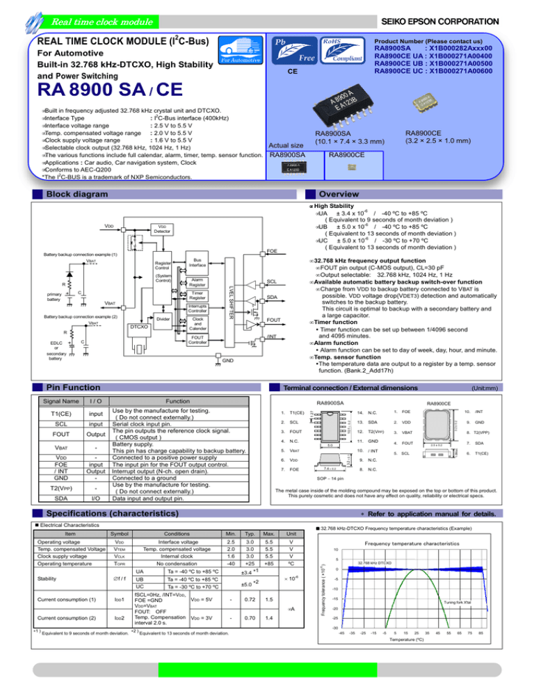
clock Real time cloc k module REAL TIME CLOCK MODULE (I2C-Bus) Product Number (Please contact us) For Automotive Built-in 32.768 kHz-DTCXO, High Stability and Power Switching RA8900SA : X1B000282Axxx00 RA8900CE UA : X1B000271A00400 RA8900CE UB : X1B000271A00500 RA8900CE UC : X1B000271A00600 CE RA 8900 SA / CE •Built in frequency adjusted 32.768 kHz crystal unit and DTCXO. 2 •Interface Type : I C-Bus interface (400kHz) •Interface voltage range : 2.5 V to 5.5 V •Temp. compensated voltage range : 2.0 V to 5.5 V •Clock supply voltage range : 1.6 V to 5.5 V Actual size •Selectable clock output (32.768 kHz, 1024 Hz, 1 Hz) •The various functions include full calendar, alarm, timer, temp. sensor function. RA8900SA •Applications : Car audio, Car navigation system, Clock •Conforms to AEC-Q200 2 *The I C-BUS is a trademark of NXP Semiconductors. RA8900CE Block diagram Overview VDD FOE VBAT Register Control (System Control) C Alarm Register Timer Register VBAT Battery backup connection example (2) VBAT Interrupts Controller Divider DTCXO Clock and Calender SCL SDA FOUT R /INT FOUT Controller C GND Pin Function VBAT - VDD FOE / INT GND input Output - T2(VPP) - SDA I/O 2. SCL 3. FOUT 4. N.C. 5. VBAT 6. VDD 7. FOE RA8900CE 14. N.C. 1. FOE 13. SDA 2. VDD 12. T2(VPP) 3. VBAT 11. GND 4. FOUT 10. / INT 5. SCL 9. N.C. 8. N.C. 5.0 7.4 ± 0.2 GND 8. T2(VPP) 2.5 ± 0.2 7. SDA 6. T1(CE) 32.768 kHz-DTCXO Frequency temperature characteristics (Example) Min. Typ. Max. Unit Operating voltage Temp. compensated Voltage Clock supply voltage Operating temperature VDD VTEM VCLK TOPR Interface voltage Temp. compensated voltage Internal clock No condensation 2.5 2.0 1.6 -40 5.5 5.5 5.5 +85 V V V ºC ∆f/f IDD1 IDD2 Equivalent to 9 seconds of month deviation. UA Ta = -40 ºC to +85 ºC 3.0 3.0 3.0 +25 ∗1 ±3.4 UB UC Ta = -40 ºC to +85 ºC Ta = -30 ºC to +70 ºC ±5.0 fSCL=0Hz, /INT=VDD, VDD = 5V FOE =GND VDD=VBAT FOUT: OFF Temp. Compensation VDD = 3V interval 2.0 s. ∗2 ) - × 10-6 ∗2 0.72 1.5 µA - 0.70 Frequency temperature characteristics 10 5 -6 Conditions Frequency tolerance ( ×10 ) Symbol ∗1 ) 9. ∗ Refer to application manual for details. Item Current consumption (2) /INT The metal case inside of the molding compound may be exposed on the top or bottom of this product. This purely cosmetic and does not have any effect on quality, reliability or electrical specs. Specifications (characteristics) Current consumption (1) 10. SOP − 14 pin Electrical Characteristics Stability 3.2 ± 0.2 input Output T1(CE) (Unit:mm) 1.0Max. SCL FOUT RA8900SA 1. 0.2 input Function Use by the manufacture for testing. ( Do not connect externally.) Serial clock input pin. The pin outputs the reference clock signal. ( CMOS output ) Battery supply. This pin has charge capability to backup battery. Connected to a positive power supply The input pin for the FOUT output control. Interrupt output (N-ch. open drain). Connected to a ground Use by the manufacture for testing. ( Do not connect externally.) Data input and output pin. 10.1 ± I/O 3.2 ± 0.1 T1(CE) Terminal connection / External dimensions 1.27 Signal Name • 32.768 kHz frequency output function • FOUT pin output (C-MOS output), CL=30 pF • Output selectable: 32.768 kHz, 1024 Hz, 1 Hz • Available automatic battery backup switch-over function • Charge from VDD to backup battery connected to VBAT is possible. VDD voltage drop(VDET3) detection and automatically switches to the backup battery. This circuit is optimal to backup with a secondary battery and a large capacitor. • Timer function Timer function can be set up between 1/4096 second and 4095 minutes. • Alarm function Alarm function can be set to day of week, day, hour, and minute. • Temp. sensor function The temperature data are output to a register by a temp. sensor function. (Bank.2_Add17h) Bus Interface LVEL SHIFTER R EDLC or secondary battery • High Stability •UA ± 3.4 x 10⁻⁶ / -40 ºC to +85 ºC ( Equivalent to 9 seconds of month deviation ) •UB ± 5.0 x 10⁻⁶ / -40 ºC to +85 ºC ( Equivalent to 13 seconds of month deviation ) -6 •UC ± 5.0 x 10 / -30 ºC to +70 ºC ( Equivalent to 13 seconds of month deviation ) VDD Detector Battery backup connection example (1) primary battery RA8900CE (3.2 × 2.5 × 1.0 mm) RA8900SA (10.1 × 7.4 × 3.3 mm) 1.4 32.768 kHz DTCXO 0 -5 -10 -15 Tuning fork X'tal -20 -25 -30 Equivalent to 13 seconds of month deviation. -45 -35 -25 -15 -5 5 15 25 Temperature (ºC) 35 45 55 65 75 85 PROMOTION OF ENVIRONMENTAL MANAGEMENT SYSTEM CONFORMING TO INTERNATIONAL STANDARDS At Seiko Epson, all environmental initiatives operate under the Plan-Do-Check-Action (PDCA) cycle designed to achieve continuous improvements. The environmental management system (EMS) operates under the ISO 14001 environmental management standard. All of our major manufacturing and non-manufacturing sites, in Japan and overseas, completed the acquisition of ISO 14001 certification. ISO 14000 is an international standard for environmental management that was established by the International Standards Organization in 1996 against the background of growing concern regarding global warming, destruction of the ozone layer, and global deforestation. WORKING FOR HIGH QUALITY In order provide high quality and reliable products and services than meet customer needs, Seiko Epson made early efforts towards obtaining ISO9000 series certification and has acquired ISO9001 for all business establishments in Japan and abroad. We have also acquired ISO/TS 16949 certification that is requested strongly by major automotive manufacturers as standard. ISO/TS16949 is the international standard that added the sector-specific supplemental requirements for automotive industry based on ISO9001. ►Explanation of the mark that are using it for the catalog ►Pb free. ►Complies with EU RoHS directive. *About the products without the Pb-free mark. Contains Pb in products exempted by EU RoHS directive. (Contains Pb in sealing glass, high melting temperature type solder or other.) ►Designed for automotive applications such as Car Multimedia, Body Electronics, Remote Keyless Entry etc. ►Designed for automotive applications related to driving safety (Engine Control Unit, Air Bag, ESC etc ). Notice • • • • • • This material is subject to change without notice. Any part of this material may not be reproduced or duplicated in any form or any means without the written permission of Seiko Epson. The information about applied data, circuitry, software, usage, etc. written in this material is intended for reference only. Seiko Epson does not assume any liability for the occurrence of customer damage or infringing on any patent or copyright of a third party. This material does not authorize the licensing for any patent or intellectual copyrights. When exporting the products or technology described in this material, you should comply with the applicable export control laws and regulations and follow the procedures required by such laws and regulations. You are requested not to use the products (and any technical information furnished, if any) for the development and/or manufacture of weapon of mass destruction or for other military purposes. You are also requested that you would not make the products available to any third party who may use the products for such prohibited purposes. These products are intended for general use in electronic equipment. When using them in specific applications that require extremely high reliability, such as the applications stated below, you must obtain permission from Seiko Epson in advance. / Space equipment (artificial satellites, rockets, etc.) / Transportation vehicles and related (automobiles, aircraft, trains, vessels, etc.) / Medical instruments to sustain life / Submarine transmitters / Power stations and related / Fire work equipment and security equipment / traffic control equipment / and others requiring equivalent reliability. • All brands or product names mentioned herein are trademarks and/or registered trademarks of their respective. Seiko Epson Corporation

