S4882
10M - 4.25Gbps Continuous Rate Transceiver
P RODUCT BR IE F
The S4882 transceiver device is a fully integrated CMOS transceiver utilizing a
single fixed rate reference clock for continuous rate coverage of the 10 Mbps
through 4.25 Gbps band. I2C/SPI accessible independent RX/TX data path rate
control, with 10 Hz resolution, also allows for asymmetrical continuous rate operation. On-chip clock synthesis and clock recovery PLL components are contained
in the S4882. The chip consists of a receive (RX) function that includes a clock
and data recovery (CDR) unit and a DeMUX. The transmit (TX) function contains
a MUX and clock synthesis unit (CSU) elements.
S48
82
USA
Features
• Serial to parallel and parallel to serial converter for
•
•
•
•
•
•
•
•
•
•
•
•
•
•
•
•
•
•
•
•
Overview
10Mbps through 4.25 Gbps with built-in CDR, CSU
and diagnostics
12.5 mV Diff Input Sensitivity at 10-12 BER
Single Reference Clock for 10 Mbps - 4.25 Gbps RX/
TX Continuous Rate Operation with 10 Hz resolution.
Single reference clock frequency for FEC and NonFEC applications.
Frame / Boundary Detection and Byte Alignment for
SONET/SDH and 8B/10B encoded protocols and
Differential RX/TX Decoding/Encoding.
Output Data De-Emphasis with Adjustable Swing
and Phase Continuous Output Clocking
Programmable Parallel Data Path (4/8/10-bit or 4-bit
Redundant Data Mode) with Optional Parity and Programmable Auto Squelch Functionality
Post Amp Offset Adjust, Loss of Signal with Run
Length Detector, Signal Detect Input, Receive Signal
Strength Indicator and RX/TX Lock Detect Output
Circuits.
Integrated PLL Loop Filter Components & I/O
Terminations for a Compact Applications
Dual REFCLK Inputs for Flexible CDR/CSU
Reference Clocking and/or External Clean-Up
Additional CDR & CSU Programmable Prescaler
Clock Outputs for Down/Upstream Timing
Transmit FIFO Depth allows for Breathing of
Transmit PCLK & PICLK Clocks
I2C & SPI Compatible Control Interfaces with Global
Alarm Interrupt, Status, and Control
Clock Multiplier Unit (CMU) Capability
Intelligent Power Down of Selected Features/Functions for Power Restricted Applications.
Recovery from Input Alarm Conditions.
1.2 V & 3.3 V Power Supply Requirements
Complies with Bellcore/ITU-T Specs for Jitter Tolerance/Transfer/Generation as well as the Related GE/
FC/CPRI/HDTV Specifications.
JTAG (IEEE 1149.1-2001 compliant) & Dual Independent Pattern Generators/Checkers
Less than 900 mW Typical Power Dissipation
Standard and Green/RoHS Compliant Lead Free
Package Options
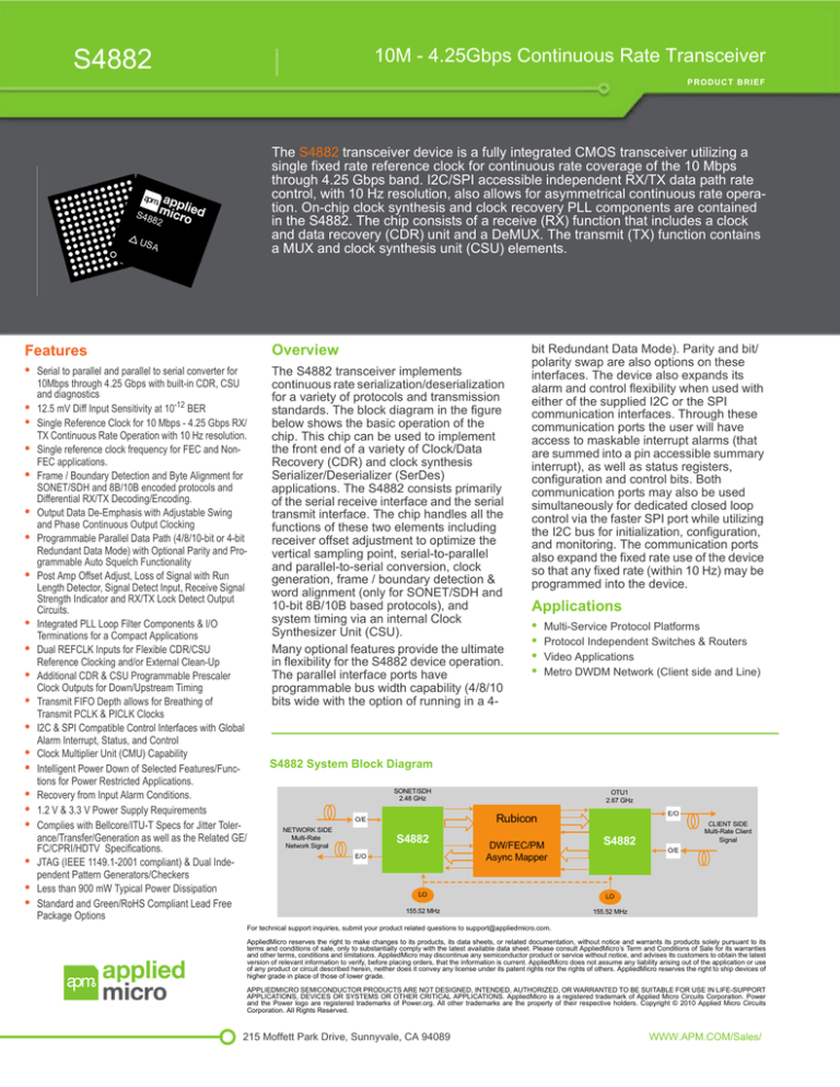
The S4882 transceiver implements
continuous rate serialization/deserialization
for a variety of protocols and transmission
standards. The block diagram in the figure
below shows the basic operation of the
chip. This chip can be used to implement
the front end of a variety of Clock/Data
Recovery (CDR) and clock synthesis
Serializer/Deserializer (SerDes)
applications. The S4882 consists primarily
of the serial receive interface and the serial
transmit interface. The chip handles all the
functions of these two elements including
receiver offset adjustment to optimize the
vertical sampling point, serial-to-parallel
and parallel-to-serial conversion, clock
generation, frame / boundary detection &
word alignment (only for SONET/SDH and
10-bit 8B/10B based protocols), and
system timing via an internal Clock
Synthesizer Unit (CSU).
Many optional features provide the ultimate
in flexibility for the S4882 device operation.
The parallel interface ports have
programmable bus width capability (4/8/10
bits wide with the option of running in a 4-
bit Redundant Data Mode). Parity and bit/
polarity swap are also options on these
interfaces. The device also expands its
alarm and control flexibility when used with
either of the supplied I2C or the SPI
communication interfaces. Through these
communication ports the user will have
access to maskable interrupt alarms (that
are summed into a pin accessible summary
interrupt), as well as status registers,
configuration and control bits. Both
communication ports may also be used
simultaneously for dedicated closed loop
control via the faster SPI port while utilizing
the I2C bus for initialization, configuration,
and monitoring. The communication ports
also expand the fixed rate use of the device
so that any fixed rate (within 10 Hz) may be
programmed into the device.
Applications
• Multi-Service Protocol Platforms
• Protocol Independent Switches & Routers
• Video Applications
• Metro DWDM Network (Client side and Line)
S4882 System Block Diagram
SONET/SDH
2.48 GHz
E/O
Rubicon
O/E
NETWORK SIDE
Multi-Rate
Network Signal
OTU1
2.67 GHz
S4882
E/O
DW/FEC/PM
Async Mapper
S4882
LO
LO
155.52 MHz
155.52 MHz
CLIENT SIDE
Multi-Rate Client
Signal
O/E
For technical support inquiries, submit your product related questions to support@appliedmicro.com.
AppliedMicro reserves the right to make changes to its products, its data sheets, or related documentation, without notice and warrants its products solely pursuant to its
terms and conditions of sale, only to substantially comply with the latest available data sheet. Please consult AppliedMicro’s Term and Conditions of Sale for its warranties
and other terms, conditions and limitations. AppliedMicro may discontinue any semiconductor product or service without notice, and advises its customers to obtain the latest
version of relevant information to verify, before placing orders, that the information is current. AppliedMicro does not assume any liability arising out of the application or use
of any product or circuit described herein, neither does it convey any license under its patent rights nor the rights of others. AppliedMicro reserves the right to ship devices of
higher grade in place of those of lower grade.
APPLIEDMICRO SEMICONDUCTOR PRODUCTS ARE NOT DESIGNED, INTENDED, AUTHORIZED, OR WARRANTED TO BE SUITABLE FOR USE IN LIFE-SUPPORT
APPLICATIONS, DEVICES OR SYSTEMS OR OTHER CRITICAL APPLICATIONS. AppliedMicro is a registered trademark of Applied Micro Circuits Corporation. Power
and the Power logo are registered trademarks of Power.org. All other trademarks are the property of their respective holders. Copyright © 2010 Applied Micro Circuits
Corporation. All Rights Reserved.
215 Moffett Park Drive, Sunnyvale, CA 94089
WWW.APM.COM/Sales/


