High-resolution group III nitride microdisplays
advertisement

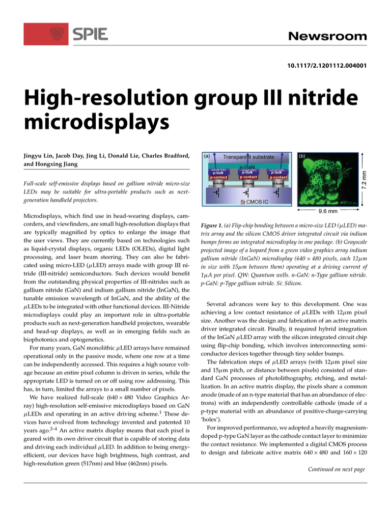
10.1117/2.1201112.004001 High-resolution group III nitride microdisplays Jingyu Lin, Jacob Day, Jing Li, Donald Lie, Charles Bradford, and Hongxing Jiang Full-scale self-emissive displays based on gallium nitride micro-size LEDs may be suitable for ultra-portable products such as nextgeneration handheld projectors. Microdisplays, which find use in head-wearing displays, camcorders, and viewfinders, are small high-resolution displays that are typically magnified by optics to enlarge the image that the user views. They are currently based on technologies such as liquid-crystal displays, organic LEDs (OLEDs), digital light processing, and laser beam steering. They can also be fabricated using micro-LED (LED) arrays made with group III nitride (III-nitride) semiconductors. Such devices would benefit from the outstanding physical properties of III-nitrides such as gallium nitride (GaN) and indium gallium nitride (InGaN), the tunable emission wavelength of InGaN, and the ability of the LEDs to be integrated with other functional devices. III-Nitride microdisplays could play an important role in ultra-portable products such as next-generation handheld projectors, wearable and head-up displays, as well as in emerging fields such as biophotonics and optogenetics. For many years, GaN monolithic LED arrays have remained operational only in the passive mode, where one row at a time can be independently accessed. This requires a high source voltage because an entire pixel column is driven in series, while the appropriate LED is turned on or off using row addressing. This has, in turn, limited the arrays to a small number of pixels. We have realized full-scale (640 480 Video Graphics Array) high-resolution self-emissive microdisplays based on GaN LEDs and operating in an active driving scheme.1 These devices have evolved from technology invented and patented 10 years ago.2–4 An active matrix display means that each pixel is geared with its own driver circuit that is capable of storing data and driving each individual LED. In addition to being energyefficient, our devices have high brightness, high contrast, and high-resolution green (517nm) and blue (462nm) pixels. Figure 1. (a) Flip-chip bonding between a micro-size LED (LED) matrix array and the silicon CMOS driver integrated circuit via indium bumps forms an integrated microdisplay in one package. (b) Grayscale projected image of a leopard from a green video graphics array indium gallium nitride (InGaN) microdisplay (640 480 pixels, each 12m in size with 15m between them) operating at a driving current of 1A per pixel. QW: Quantum wells. n-GaN: n-Type gallium nitride. p-GaN: p-Type gallium nitride. Si: Silicon. Several advances were key to this development. One was achieving a low contact resistance of LEDs with 12m pixel size. Another was the design and fabrication of an active matrix driver integrated circuit. Finally, it required hybrid integration of the InGaN LED array with the silicon integrated circuit chip using flip-chip bonding, which involves interconnecting semiconductor devices together through tiny solder bumps. The fabrication steps of LED arrays (with 12m pixel size and 15m pitch, or distance between pixels) consisted of standard GaN processes of photolithography, etching, and metallization. In an active matrix display, the pixels share a common anode (made of an n-type material that has an abundance of electrons) with an independently controllable cathode (made of a p-type material with an abundance of positive-charge-carrying ‘holes’). For improved performance, we adopted a heavily magnesiumdoped p-type GaN layer as the cathode contact layer to minimize the contact resistance. We implemented a digital CMOS process to design and fabricate active matrix 640 480 and 160 120 Continued on next page 10.1117/2.1201112.004001 Page 2/2 microdisplay controller integrated circuits. These circuits have a LED current of 0.5–10A and the same pitch of 15m as the LED array. Figure 1(a) shows the interconnection between the array and the silicon CMOS driver integrated circuit accomplished by flip-chip bonding using indium bumps 6m in size, which were deposited by thermal evaporation. The hybrid integration means that thousands of signal connections between the microdisplay and the driving circuit have been established in a single flip-chip bonding package. The measured luminance level of the microdisplays is much higher than that of LCD and OLED devices. Figure 1(b) shows a grayscale projected image of a leopard from a green InGaN microdisplay with 640 480 pixels. The device is fully compatible with current video graphics technology. The pixel emission intensity was almost constant over an operational temperature range from 100 to 100ı C. The outstanding performance is a direct attribute of III-nitride semiconductors. We intend to optimize the prototype device for commercialization. A Small Business Innovation Research contract from the US Army Night Vision and Electronic Sensors Directorate made our recent advances possible. Author Information at the TTU Health Sciences Center and an associate editor of IEEE Microwave and Wireless Components Letters. Hongxing Jiang is the Edward Whitacre Endowed Chair and Professor of electrical and computer engineering. He has over 300 scientific publications (with 5700 citations and an h-index of 42) and holds 20 patents. He relocated in 2008 from KSU where he was a distinguished professor. He is an American Physical Society fellow. Jing Li III-N Technology Inc. Lubbock, TX Jing Li received a PhD in physics from KSU in 2003. He is currently serving as an R&D director at III-N Technology Inc. He has published over 50 journal papers and holds five patents. Charles Bradford US Army Research, Development, and Engineering Command Communications-Electronic Research, Development, and Engineering Center Night Vision and Electronic Sensors Directorate Ft. Belvoir, VA References Jingyu Lin, Jacob Day, Donald Lie, and Hongxing Jiang Department of Electrical and Computer Engineering Texas Tech University (TTU) Lubbock, TX Jingyu Lin is the Linda Whitacre Endowed Chair and Professor of electrical and computer engineering. She has over 300 scientific publications (with 5600 citations and an h-index of 42) and holds 20 patents. She relocated in 2008 from Kansas State University (KSU) where she was a professor of physics. 1. J. Day, J. Li, D. Y. C. Lie, C. Bradford, J. Y. Lin, and H. X. Jiang, III-Nitride full-scale high-resolution microdisplays, Appl. Phys. Lett. 99, p. 031116, 2011. 2. S. X. Jin, J. Li, J. Z. Li, J. Y. Lin, and H. X. Jiang, GaN microdisk light emitting diodes, Appl. Phys. Lett. 76, p. 631, 1999. 3. H. X. Jiang, S. X. Jin, J. Li, J. Shakya, and J. Y. Lin, III-nitride blue microdisplays, Appl. Phys. Lett. 78, p. 1303, 2001. 4. H. X. Jiang, S. X. Jin, J. Li, and J. Y. Lin, Micro-size LED and detector arrays for minidisplay, hyper-bright light emitting diodes, lighting, and UV detector and imaging sensor applications, US Patent 6,410,940, 2002. Jacob Day received his BS and PhD from Texas Tech University (2006 and 2011, respectively). He currently works as a senior analog integrated circuits designer at Texas Instruments Inc., Dallas, TX. His research interests include the design of analog integrated circuits such as DC-DC converters and peripherals necessary for power management systems-on-chip. Donald Y. C. Lie is the K. S. Lu Regents Endowed Chair and associate professor of electrical and computer engineering. He has over 120 peer-reviewed publications and holds five US patents. He is also an adjunct associate professor of surgery c 2011 SPIE


