Dec 2003 Save Board Space with a High Efficiency Dual
advertisement
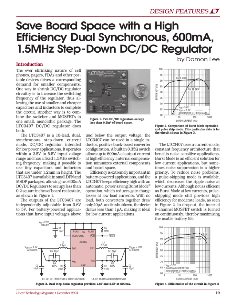
DESIGN FEATURES Save Board Space with a High Efficiency Dual Synchronous, 600mA, 1.5MHz Step-Down DC/DC Regulator by Damon Lee Introduction 100 The ever shrinking nature of cell phones, pagers, PDAs and other portable devices drives a corresponding demand for smaller components. One way to shrink DC/DC regulator circuitry is to increase the switching frequency of the regulator, thus allowing the use of smaller and cheaper capacitors and inductors to complete the circuit. Another way is to combine the switcher and MOSFETs in one small, monolithic package. The LTC3407 DC/DC regulator does both. The LTC3407 is a 10-lead, dual, synchronous, step-down, current mode, DC/DC regulator, intended for low power applications. It operates within a 2.5V to 5.5V input voltage range and has a fixed 1.5MHz switching frequency, making it possible to use tiny capacitors and inductors that are under 1.2mm in height. The LTC3407 is available in small DFN and MSOP packages, allowing two 600mA DC/DC Regulators to occupy less than 0.2 square inches of board real estate, as shown in Figure 1. The outputs of the LTC3407 are independently adjustable from 0.6V to 5V. For battery-powered applications that have input voltages above 95 VOUT2 = 2.5V AT 600mA C3 10µF C5, 22pF R4 887k EFFICIENCY (%) and below the output voltage, the LTC3407 can be used in a single inductor, positive buck-boost converter configuration. A built in 0.35Ω switch allows up to 600mA of output current at high efficiency. Internal compensation minimizes external components and board space. Efficiency is extremely important in battery-powered applications, and the LTC3407 keeps efficiency high with an automatic, power saving Burst Mode® operation, which reduces gate charge losses at low load currents. With no load, both converters together draw only 40µA, and in shutdown, the device draws less than 1µA, making it ideal for low current applications. VIN RUN1 SW1 VFB2 VFB1 GND 10 100 LOAD CURRENT (mA) 1000 The LTC3407 uses a current-mode, constant frequency architecture that benefits noise sensitive applications. Burst Mode is an efficient solution for low current applications, but sometimes noise suppression is a higher priority. To reduce noise problems, a pulse-skipping mode is available, which decreases the ripple noise at low currents. Although not as efficient as Burst Mode at low currents, pulseskipping mode still provides high efficiency for moderate loads, as seen in Figure 2. In dropout, the internal P-channel MOSFET switch is turned on continuously, thereby maximizing the usable battery life. 95 RESET C4, 22pF R2 R1 887k 442k 2.5V 90 VOUT1 = 1.8V AT 600mA 1.8V 85 80 75 70 C2 10µF L1, L2: MURATA LQH32CN2R2M33 Figure 3. Dual step-down regulator provides 1.8V and 2.5V at 600mA. VIN = 3.3V Burst Mode OPERATION NO LOAD ON OTHER CHANNEL 65 60 C1, C2, C3: TAIYO YUDEN JMK316BJ106ML 1 100 L1 2.2µH SW2 Linear Technology Magazine • December 2003 VIN = 3.6V VOUT = 1.8V NO LOAD ON OTHER CHANNEL Figure 2. Comparison of Burst Mode operation and pulse skip mode. This particular data is for the circuit shown in Figure 3. R5 100k POR LTC3407 R3 280k 75 60 Figure 1. Two DC/DC regulators occupy less than 0.2in2 of board space. MODE/SYNC L2 2.2µH PULSE SKIP 80 65 EFFICIENCY (%) RUN2 85 70 VIN = 2.5V TO 5.5V C1 10µF Burst Mode 90 1 10 100 LOAD CURRENT (mA) 1000 Figure 4. Efficiencies of the circuit in Figure 3 19 DESIGN FEATURES VIN = 2.8V TO 4.2V C1 10µF RUN2 VIN RUN1 MODE/SYNC VOUT2 = 3.3V AT 200mA RESET POR LTC3407 L2 10µH D1 L1 2.2µH SW1 SW2 C6 47µF R4 887k R3 196k C3 10µF C1, C2, C3: TAIYO YUDEN JMK316BJ106ML C6: SANYO 6TPB47M D1: PHILIPS PMEG2010 VFB1 VFB2 VOUT1 = 1.8V AT 600mA C4, 22pF M1 + when using only ceramic input and output capacitors. The LTC3407 was designed with ceramic capacitors in mind and is internally compensated to handle these difficult design considerations. High quality X5R or X7R ceramic capacitors should be used to minimize the temperature and voltage coefficients. Figure 3 shows a typical application for the LTC3407 using only ceramic capacitors. This circuit provides a regulated 2.5V output and a regulated 1.8V output, both at up to 600mA, from a 2.5V to 5.5V input. Efficiency for the circuit is as high as 95% as shown in Figure 4. R5 100k R2 R1 887k 442k GND C2 10µF L1: MURATA LQH32CN2R2M33 L2: TOKO A914BYW-100M (D52LC SERIES) M1: SILICONIX Si2302 Figure 5. Single inductor, positive buck-boost regulator and a buck regulator with maximum height < 2mm 90 100 95 2.8V 3.6V 60 50 2.8V 2mm Height Li-Ion, Single Inductor, Buck-Boost Regulator and Buck Regulator 3.6V 90 4.2V 70 EFFICIENCY (%) EFFICIENCY (%) 80 4.2V 85 Lithium-Ion batteries are popular in many portable applications because of their light weight and high energy density, but the battery voltage ranges from a fully charged 4.2V down to a drained 2.8V. When a device requires an output voltage that falls somewhere in the middle of the Li-Ion operating range, such as the 3.3V I/O supply, a simple buck or boost converter does not work. One solution is a single inductor, positive buck-boost regulator, which allows the input voltage to vary above and below the output voltage. In Figure 5, regulator 2 is configured as a single inductor, positive buckboost regulator to supply a constant 3.3V with 200mA–400mA of load current, depending on the battery voltage. The circuit is well suited to portable 80 75 70 40 30 65 VOUT = 3.3V Burst Mode OPERATION 1 10 100 LOAD CURRENT (mA) 1000 60 VOUT = 1.8V Burst Mode OPERATION 1 10 100 LOAD CURRENT (mA) 1000 Figure 6. Efficiencies for the circuit in Figure 4 A Power-On Reset (POR) output is available for microprocessor systems to insure proper startups. Internal overvoltage and undervoltage comparators on both outputs will pull the POR output low if the output voltages are not within ±8.5%. The POR output is delayed by 262,144 clock cycles (about 175ms) after achieving regulation, but will be pulled low immediately when either ouput is out of regulation. phase margin. Ceramic capacitors, on the other hand, remain capacitive to beyond 300kHz and usually resonate with their ESL before the ESR becomes effective. Also, inexpensive ceramic capacitors are prone to temperature and voltage effects, requiring the designer to check loop stability over the operating temperature range. For these reasons, great care is usually needed High Efficiency 2.5V and 1.8V Step-Down DC/DC Regulator with all Ceramic Capacitors The low cost and low ESR of ceramic capacitors make them a very attractive choice for use in switching regulators. In addition, ceramic capacitors have a benign failure mechanism unlike tantalum capacitors. Unfortunately, the ESR is so low that it can cause loop stability issues. A solid tantalum capacitor’s ESR generates a loop zero at 5kHz–50kHz that can be instrumental in giving acceptable loop 20 VIN = 2.8V TO 4.2V C1 2×4.7µF RUN2 VIN MODE/SYNC VOUT2 = 2.5V AT 600mA C3 2×4.7µF R4 887k SW2 VFB1 C1, C2, C3: TDK C1608X5ROJ475M GND RESET L1 2.2µH SW1 VFB2 R3 280k R5 100k POR LTC3407 L2 2.2µH C5, 22pF RUN1 C4, 22pF R2 R1 604k 402k VOUT1 = 1.5V AT 600mA C2 2×4.7µF L1, L2: SUMIDA CDRH2D11-2.2µH Figure 6. Low profile (1.2mm) Lithium-Ion dual step-down regulator Linear Technology Magazine • December 2003 DESIGN FEATURES 100 100 95 95 2.8V 90 4.2V 85 EFFICIENCY (%) EFFICIENCY (%) 90 3.6V 80 75 70 4.2V 85 3.6V 80 75 70 VOUT = 1.5V Burst Mode OPERATION NO LOAD ON OTHER CHANNEL 65 60 2.8V 1 10 100 LOAD CURRENT (mA) VOUT = 2.5V Burst Mode OPERATION NO LOAD ON OTHER CHANNEL 65 60 1000 1 10 100 LOAD CURRENT (mA) 1000 Figure 7. Efficiencies for the circuit in Figure 6 applications because none of the components exceed 2mm in height. The efficiency varies with the input supply, due to resistive losses at high currents and to switching losses at low currents. As shown in Figure 6, the typical efficiency across both battery voltage and load current is about 75% for the 3.3V output, and about 90% for the 1.8V output. Power over Ethernet, continued from page 18 These changes do add diodes to the PD, but it’s definitely for the best. Thanks to Auto-MDI-X, today’s Ethernet switches and routers work equally well with or without crossover cables. Because the PD now must also accept power of either polarity, 802.3af Power over Ethernet will work with either type of cable, minimizing end user confusion. The 802.3af standard now defines specific peak currents for class 1 and 2 PDs. While all PDs can draw 400mA of inrush current when they are first powered, current consumption thereafter depends on the class of the PD. height requirement, and to occupy less than 0.2in2. The circuit provides 2.5V and 1.5V outputs, each with up to 600mA of load current. Two 4.7µF ceramic capacitors are used on each supply, due to the lack of availability of low profile 10µF ceramic capacitors. The efficiency is slightly lower due to the higher series resistance of the low profile inductors. A peak efficiency of 91% for the 1.5V output and 95% for the 2.5V output is achieved with these components, as seen in Figure 7. Low Profile, 1.2mm Height, Lithium-Ion Dual Supply Conclusion In some applications, minimizing the height of the circuit takes prime importance. New low profile capacitors and inductors can be combined with the already low profile 1.1mm maximum height of the LTC3407’s 10-lead MSOP package. Figure 6 shows a circuit designed to meet a 1.2mm maximum The LTC3407 is a dual monolithic, step-down regulator that switches at 1.5MHz, minimizing component costs and board real estate requirements for DC/DC regulators. The small size, efficiency, low external component count, and design flexibility of the LTC3407 make it ideal for portable applications. Class 0 and 3 PDs must still never draw more than 400mA peak and 350mA continuous. Class 1 PDs cannot exceed 120mA peak and consume more than 3.84W continuously and Class 2 PDs must limit their peak current to 210mA and continuously use no more than 6.49W. These peak current limits do not require a class 1 or 2 PD to include active current limiting (unless it has more than 180µF of input bypass) as long as its switching regulator stays below the average power limit and filtering keeps peak currents below the specified maximum. While the standard does not specifically ad- dress this point, a PD does not have to stay below these peak limits if VPORT suddenly increases. Furthermore, the standard does not allow a PSE to apply a lower active current limit, ILIM, based on a PD’s class. A PSE, however, may monitor the PD’s current and decide to disconnect it if PD is not staying within the limits of its class, i.e. the PSE may reduce the ICUT threshold for a class 1 or 2 PD. In addition to the changes listed above there are some minor parametric changes. Refer to the IEEE 802.3af-2003 standard for further details. + OR – FROM SIGNAL PAIRS + OR – + + OR – FROM SPARE PAIRS – LTC4257 GND SMAJ58A RCLASS SIGDISA C1 RPULLUP 4.7µF 51k 100V PWRGD RCLASS VIN VOUT + VIN SWITCHING POWER SUPPLY SHDN GND + 3.3V TO LOGIC – + OR – Figure 4. Typical PD application Linear Technology Magazine • December 2003 21
