GTV358
1MHz, 1.8V, CMOS,
Rail-to-Rail Dual Operational Amplifier
Advanced
1. Features
Single-Supply Operation from +1.8V ~ +5.5V
Low Offset Voltage: 5mV (Max.)
Rail-to-Rail Input / Output
Quiescent Current: 55μA per Amplifier (Typ.)
Gain-Bandwidth Product: 1MHz (Typ.)
Operating Temperature: -40°C ~ +125°C
Low Input Bias Current: 10pA (Typ.)
Available in SOP8 and MSOP8 Packages
2. General Description
The GTV358 is a single supply, low power CMOS dual operational amplifier; these amplifiers offer bandwidth of 1MHz, rail-to-rail
inputs and outputs, and single-supply operation from 1.8V to 5.5V. Typical low quiescent supply current of 110μA in dual
operational amplifiers within one chip and very low input bias current of 10pA make the devices an ideal choice for low offset, low
power consumption and high impedance applications such as smoke detectors, photodiode amplifiers, and other sensors.
o
o
The GTV358 is available in SOP8 and MSOP8 packages. The extended temperature range of -40 C to +125 C over all supply
voltages offers additional design flexibility.
3. Applications
Portable Equipment
Medical Instrumentation
Mobile Communications
Battery-Powered Instruments
Smoke Detector
Handheld Test Equipment
Sensor Interface
4. Pin Configuration
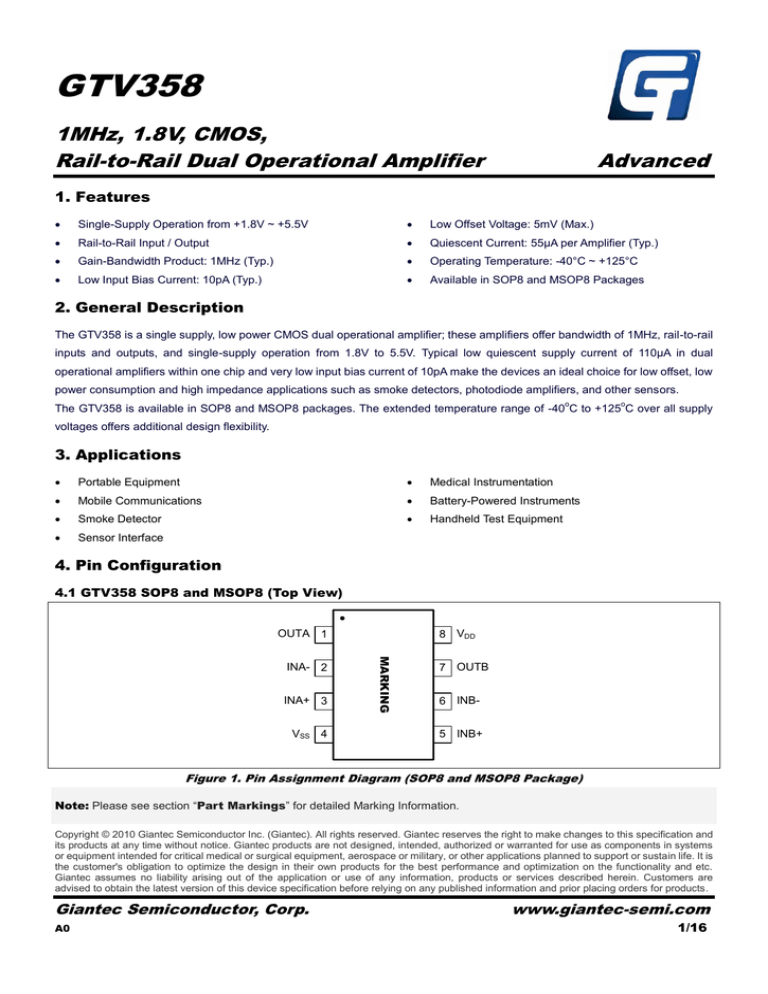
4.1 GTV358 SOP8 and MSOP8 (Top View)
OUTA 1
INA+ 3
VSS 4
MARKING
INA- 2
8 VDD
7 OUTB
6 INB5 INB+
Figure 1. Pin Assignment Diagram (SOP8 and MSOP8 Package)
Note: Please see section “Part Markings” for detailed Marking Information.
Copyright © 2010 Giantec Semiconductor Inc. (Giantec). All rights reserved. Giantec reserves the right to make changes to this specification and
its products at any time without notice. Giantec products are not designed, intended, authorized or warranted for use as components in systems
or equipment intended for critical medical or surgical equipment, aerospace or military, or other applications planned to support or sustain life. It is
the customer's obligation to optimize the design in their own products for the best performance and optimization on the functionality and etc.
Giantec assumes no liability arising out of the application or use of any information, products or services described herein. Customers are
advised to obtain the latest version of this device specification before relying on any published information and prior placing orders for products.
Giantec Semiconductor, Corp.
A0
www.giantec-semi.com
1/16
GTV358
5. Application Information
5.1 Size
GTV358 series op amps are unity-gain stable and suitable for a wide range of general-purpose applications. The small
footprints of the GTV358 series packages save space on printed circuit boards and enable the design of smaller electronic
products.
5.2 Power Supply Bypassing and Board Layout
GTV358 series operates from a single 1.8V to 5.5V supply or dual ±0.9V to ±2.75V supplies. For best performance, a 0.1μF
ceramic capacitor should be placed close to the VDD pin in single supply operation. For dual supply operation, both V DD and VSS
supplies should be bypassed to ground with separate 0.1μF ceramic capacitors.
5.3 Low Supply Current
The low supply current (typical 110μA) of GTV358 series will help to maximize battery life. They are ideal for battery powered
systems
5.4 Operating Voltage
GTV358 series operate under wide input supply voltage (1.8V to 5.5V). In addition, all temperature specifications apply from
o
o
-40 C to +125 C. Most behavior remains unchanged throughout the full operating voltage range. These guarantees ensure
operation throughout the single Li-Ion battery lifetime
5.5 Rail-to-Rail Input
The input common-mode range of GTV358 series extends 100mV beyond the supply rails (V SS-0.1V to VDD+0.1V). This is
achieved by using complementary input stage. For normal operation, inputs should be limited to this range.
5.6 Rail-to-Rail Output
Rail-to-Rail output swing provides maximum possible dynamic range at the output. This is particularly important when
operating in low supply voltages. The output voltage of GTV358 series can typically swing to less than 10mV from supply rail in
light resistive loads (>100kΩ), and 60mV of supply rail in moderate resistive loads (10kΩ).
5.7 Capacitive Load Tolerance
The GTV358 series can directly drive 250pF capacitive load in unity-gain without oscillation. Increasing the gain enhances the
amplifier’s ability to drive greater capacitive loads. In unity-gain configurations, the capacitive load drive can be improved by
inserting an isolation resistor RISO in series with the capacitive load, as shown in Figure 2.
-
RISO
VOUT
VIN
+
CL
Figure 2. Indirectly Driving a Capacitive Load Using Isolation Resistor
The bigger the RISO resistor value, the more stable VOUT will be. However, if there is a resistive load RL in parallel with the
capacitive load, a voltage divider (proportional to RISO/RL) is formed, this will result in a gain error.
The circuit in Figure 3 is an improvement to the one in Figure 2. RF provides the DC accuracy by feed-forward the VIN to RL. CF
and RISO serve to counteract the loss of phase margin by feeding the high frequency component of the output signal back to the
amplifier’s inverting input, thereby preserving the phase margin in the overall feedback loop. Capacitive drive can be increased
Giantec Semiconductor, Corp.
A0
www.giantec-semi.com
2/16
GTV358
by increasing the value of CF. This in turn will slow down the pulse response.
CF
RF
RISO
-
VOUT
VIN
+
CL
RL
Figure 3. Indirectly Driving a Capacitive Load with DC Accuracy
5.8 Differential amplifier
The differential amplifier allows the subtraction of two input voltages or cancellation of a signal common the two inputs. It is useful
as a computational amplifier in making a differential to single-end conversion or in rejecting a common mode signal. Figure 4.
shown the differential amplifier using GTV358.
R2
R1
VIN
R3
VIP
VOUT
+
R4
VREF
Figure 4. Differential Amplifier
VOUT ( RR13RR24 ) RR14 VIN
R2
V ( RR13RR24 ) RR13 VREF
R1 IP
If the resistor ratios are equal (i.e. R1=R3 and R2=R4), then
VOUT
R2
R1
(VIP VIN ) VREF
5.9 Instrumentation Amplifier
The input impedance of the previous differential amplifier is set by the resistors R1, R2, R3, and R4. To maintain the high input
impedance, one can use a voltage follower in front of each input as shown in the following two instrumentation amplifiers.
5.10 Three-Op-Amp Instrumentation Amplifier
The dual GTV358 can be used to build a three-op-amp instrumentation amplifier as shown in Figure 5.
Giantec Semiconductor, Corp.
A0
www.giantec-semi.com
3/16
GTV358
R2
R1
VIM
+
VOUT
VIP
+
R3
+
-
R4
VREF
Figure 5. Three-Op-Amp Instrumentation Amplifier
The amplifier in Figure 5 is a high input impedance differential amplifier with gain of R 2/R1. The two differential voltage followers
assure the high input impedance of the amplifier.
Vo (1
R4
R3
)(VIP VIN )
5.11 Two-Op-Amp Instrumentation Amplifier
GTV358 can also be used to make a high input impedance two-op-amp instrumentation amplifier as shown in Figure 6.
R2
R4
R1
VIM
R3
+
VOUT
VIP
+
Figure 6. Two-Op-Amp Instrumentation Amplifier
Where R1=R3 and R2=R4. If all resistors are equal, then Vo=2(VIP-VIN)
Giantec Semiconductor, Corp.
A0
www.giantec-semi.com
4/16
GTV358
5.12 Single-Supply Inverting Amplifier
The inverting amplifier is shown in Figure 6. The capacitor C 1 is used to block the DC signal going into the AC signal source V IN.
The value of R1 and C1 set the cut-off frequency to ƒC=1/(2πR1C1). The DC gain is defined by VOUT=-(R2/R1)VIN
R2
C1
R1
VIN
R3
VOUT
VIP
+
R4
Figure 7. Single Supply Inverting Amplifier
5.13 Low Pass Active Filter
The low pass active filter is shown in Figure 8. The DC gain is defined by –R2/R1. The filter has a -20dB/decade roll-off after
its corner frequency ƒC=1/(2πR3C1).
C1
R2
R1
VIN
VOUT
+
R3
Figure 8. Low Pass Active Filter
5.14 Sallen-Key 2nd Order Active Low-Pass Filter
GTV358 can be used to form a 2
nd
order Sallen-Key active low-pass filter as shown in Figure 9. The transfer function from VIN to
VOUT is given by
VOUT
VIN
(S )
1
C1C2 R1R2
ALP
S 2 S ( C 1R C 1R C 1R C LPR ) C C 1R R
A
1 1
1 2
2 2
2 2
1 2 1 2
Where the DC gain is defined by ALP=1+R3/R4, and the corner frequency is given by
C
1
C1C2R1R2
The pole quality factor is given by
Giantec Semiconductor, Corp.
A0
www.giantec-semi.com
5/16
GTV358
C
Q
1
C1R1
C11R2 C21R2 CA2LPR2
Let R1=R2=R and C1=C2=C, the corner frequency and the pole quality factor can be simplified as below
C CR1
And Q=2-R3/R4
C1
R1
R2
-
VIN
VOUT
C2
+
R3
R4
Figure 9. Sanllen-Key 2nd Order Active Low-Pass Filter
5.15 Sallen-Key 2
nd
The 2
nd
Order high-Pass Active Filter
order Sallen-key high-pass filter can be built by simply interchanging those frequency selective components R1, R2, C1,
and C2 as shown in Figure 10.
R1
C1
C2
VIN
VOUT
R2
+
R3
R4
Figure 10. Sanllen-Key 2nd Order Active High-Pass Filter
VOUT
VIN
(S )
S 2 AHP
S 2 S ( C 1R C 1R
1 1
2 2
1 AHP
) C C 1R R
C1R1
1 2 1 2
Where AHP=1+R3/R4
Giantec Semiconductor, Corp.
A0
www.giantec-semi.com
6/16
GTV358
6. Electrical Characteristics
6.1 Absolute Maximum Ratings
Condition
Min
Max
-0.5V
+7V
Analog Input Voltage (IN+ or IN-)
Vss-0.5V
VDD+0.5V
PDB Input Voltage
Vss-0.5V
+7V
-40°C
+125°C
Power Supply Voltage (VDD to Vss)
Operating Temperature Range
Junction Temperature
Storage Temperature Range
Lead Temperature (soldering, 10sec)
+150°C
-65°C
+150°C
+300°C
Package Thermal Resistance (TA=+25℃)
SOP8, θJA
130°C
MSOP8, θJA
210°C
Note: Stress greater than those listed under Absolute Maximum Ratings may cause permanent damage to the device. This is a
stress rating only and functional operation of the device at these or any other conditions outside those indicated in the operational
sections of this specification are not implied. Exposure to absolute maximum rating conditions for extended periods may affect
reliability.
Giantec Semiconductor, Corp.
A0
www.giantec-semi.com
7/16
GTV358
6.2 Electrical Characteristics
(VDD = +5V, Vss = 0V, VCM = 0V, VOUT = VDD/2, RL=100K tied to VDD/2, SHDNB = VDD, TA = -40°C to
+125°C, unless otherwise noted. Typical values are at T A =+25°C.) (Notes 1)
Parameter
Symbol
Min.
Typ.
Max.
Units
1.8
-
5.5
V
-
55
80
μA
VOS
-
0.5
5
mV
ΔVOS/ΔT
-
2
-
μV/°C
Supply-Voltage Range
Guaranteed by the PSRR test
VDD
Quiescent Supply Current (per
Amplifier)
Input Offset Voltage
Input Offset Voltage Tempco
Conditions
VDD = 5V
Input Bias Current
IB
(Note 2)
-
10
-
pA
Input Offset Current
IOS
(Note 2)
-
10
-
pA
-0.1
-
VDD+0.1
V
VDD=5.5 Vss-0.1VVCMVDD+0.1V
60
75
-
dB
Vss≤VCM≤5V
65
80
-
dB
VDD = +1.8V to +5.5V
75
90
-
dB
90
100
-
dB
65
75
-
dB
Input Common-Mode Voltage
VCM
Range
Common-Mode Rejection Ratio
CMRR
Power-Supply Rejection Ratio
PSRR
Open-Loop Voltage Gain
AV
VDD=5V, RL=100k,
0.05V≤VO≤4.95V
VDD=5V, RL=5k,
0.05V≤VO≤4.95V
Output Voltage Swing
|VIN+-VIN-| 10mV
VDD-VOH
-
6
-
mV
RL = 100k to VDD/2
VOL-VSS
-
6
-
mV
|VIN+-VIN-| 10mV
VDD-VOH
-
60
-
mV
RL = 5k to VDD/2
VOL-VSS
-
60
-
mV
Sinking or Sourcing
-
20
-
mA
GBW
AV = +1V/V
-
1
-
MHz
SR
AV = +1V/V
-
0.6
-
V/μs
-
5
-
μs
VIN Gain=VS
-
2
-
μs
ƒ = 1kHz
-
50
-
nV/Hz
ƒ = 10kHz
-
20
-
nV/Hz
VOUT
Output Short-Circuit Current
ISC
Gain Bandwidth Product
Slew Rate
Settling Time
tS
To 0.1%, VOUT = 2V step
AV = +1V/V
Over Load Recovery Time
Input Voltage Noise Density
en
Note 1: All devices are 100% production tested at TA = +25°C; all specifications over the automotive temperature range is
guaranteed by design, not production tested.
Note 2: Parameter is guaranteed by design.
Giantec Semiconductor, Corp.
A0
www.giantec-semi.com
8/16
GTV358
6.3 Typical characteristics
At TA=+25°C, RL=100 kΩ connected to VS/2 and VOUT= VS/2, unless otherwise noted.
Large Signal Step Response
G=+1V/V,RL=100kΩ,CL=100pF
G=+1V/V,RL=100kΩ,CL=100pF
100mV/div
500mV/div
Small Signal Step Response
10μs/div
2μs/div
Large Signal Step Response
G=-1V/V,RL=100 kΩ,CL=100pF
0V 0.5V
1V/div
-2.5V
0V
Overload Recovery Time
10μs/div
Input Voltage noise Spectral Density VS. Frequency
Input Voltage noise Spectral Density VS. Frequency
Noise Gain=+10,Vn=26(nV/√HZ)@10kHz
Noise Gain=+10,Vn=51(nV/√HZ)@1kHz
10dBm/div
10dBm/div
2μs/div
2kHz/div
Giantec Semiconductor, Corp.
A0
2kHz/div
www.giantec-semi.com
9/16
GTV358
At TA=+25°C, RL=100 kΩ connected to VS/2 and VOUT= VS/2, unless otherwise noted.
Output Voltage Swing vs. Output Current
Output Voltage Swing vs. Output Current
Vs=3V
Output Voltage(V)
Output Voltage(V)
Vs=5V
Sourcing Current
Sinking Current
Output Current(mA)
Sourcing Current
Sinking Current
Output Current(mA)
Quiescent and Short-Circuit Current Vs. Supply
Small Signal Overshoot vs. Load Capacitance
IQ
ISC
Small Signal Overshoot(%)
Short circuit Current (mA)
Quiescent Current (uA)
Voltage
Supply Voltage (V)
G=-1V/V, RL=100KΩ
G=+1V/V, RL=100KΩ
Load Capacitance(pF)
Supply Current vs. Temmperature
Open-Loop Gain And Phase VS. Frequency
Frequency (Hz)
Giantec Semiconductor, Corp.
A0
Supply Current(uA)
Gain
Phase (ͦ )
Open-Loop Gain (dB)
Phase
Vs=5V
Vs=3V
Vs=1.8
V
Temperature(°C)
www.giantec-semi.com
10/16
GTV358
7. Ordering Information
GT
V
XXX
-
XX
X
X
Temperature Range
I
Industrial: -40°C~+125°C
Pb Status
G
GREEN
Package Type:
G
SOP
S
MSOP
Part Number
Low Voltage: 1.8V
Giantec Prefix
GT
Giantec
Order Number
Package Description
Package Option
GTV358-GGI-TR
SOP8
Tape and Reel 4000
GTV358-SGI-TR
MSOP8
Tape and Reel 4000
Giantec Semiconductor, Corp.
A0
www.giantec-semi.com
11/16
GTV358
8. Part Markings
8.1 GTV358-GGI (Top View)
G
T
V
3
5
8
G
G
W
S
V
I
Lot Number
Y
Y
W
GTV358GGI
Lot Number
States the last 9 characters of the wafer lot information
Pin 1 Indicator
YY
Seal Year
00 = 2000
01 = 2001
99 = 2099
WW
Seal Week
01 = Week 1
02 = Week 2
.
.
.
51 = Week 51
52 = Week 52
S
Subcon Code
J = ASESH
L = ASEKS
V
Die Version
Giantec Semiconductor, Corp.
A0
www.giantec-semi.com
12/16
GTV358
8.2 GTV358-SGI (Top View)
G
T
V
3
5
8
Lot Number
Y
Y
W
W
GTV358
GTV358-SGI
Lot Number
States the last 9 characters of the wafer lot information
Pin 1 Indicator
YY
Seal Year
S
V
00 = 2000
01 = 2001
99 = 2099
WW
Seal Week
01 = Week 1
02 = Week 2
.
.
.
51 = Week 51
52 = Week 52
S
Subcon Code
J = ASESH
L = ASEKS
V
Die Version
Giantec Semiconductor, Corp.
A0
www.giantec-semi.com
13/16
GTV358
9. Package Information
9.1 SOP8
Detail A
D
E
E1
b
ZD
Detail A
GAUGE
PLANE
A
SEATING
PLANE
e
SYMBOLS
A1
DIMENSIONS IN MILLIMETERS
Θ
DIMENSIONS IN INCHES
MIN
NOM
MAX
MIN
NOM
MAX
A
1.35
--
1.75
0.053
--
0.069
A1
0.10
--
0.25
0.004
--
0.010
b
0.33
--
0.51
0.013
--
0.020
D
4.80
--
5.00
0.189
--
0.197
Note:
E
5.80
--
6.20
0.228
--
0.244
1. Controlling Dimension:MM
E1
3.80
--
4.00
0.150
--
0.157
2. Dimension D and E1 do not include
Mold protrusion
3. Dimension b does not include
dambar protrusion/intrusion.
4. Refer to Jedec standard MS-012
5. Drawing is not to scale
e
L
1.27 BSC.
0.38
L1
Θ
--
0.050 BSC.
1.27
0.015
0.25 BSC.
ZD
0.545 REF.
0
--
0.050
0.010 BSC.
0.021 REF.
8°
Giantec Semiconductor, Corp.
A0
L
L1
0
--
8°
www.giantec-semi.com
14/16
GTV358
9.2 MSOP8
D
C
e
L
E
12°(4X)
E1
A2
θ
A
A1
b
SYMBOLS
A
A1
A2
b
C
D
E
E1
e
L
Θ
DIMENSIONS IN MILLIMETERS
MIN
-0.05
0.75
0.25
0.13
2.90
2.90
-0
NOM
--0.85
--3.00
3.00
4.90 BSC
0.65 BSC
---
DIMENSIONS IN INCHES
MAX
1.10
0.15
0.95
0.40
0.23
3.10
3.10
MIN
-0.002
0.030
0.010
0.005
0.114
0.114
0.55
7°
-0
NOM
--0.033
--0.118
0.118
0.193 BSC
0.026 BSC
---
MAX
0.043
0.006
0.037
0.016
0.009
0.122
0.122
0.022
7°
Note:
1. Controlling Dimension:MM
2. Dimension D and E1 do not include Mold protrusion
3. Refer to Jedec standard MO187
4. Drawing is not to scale
Giantec Semiconductor, Corp.
A0
www.giantec-semi.com
15/16
GTV358
10. Revision History
Revision
Date
Descriptions
A0
Oct.,2011
Initial Version
Giantec Semiconductor, Corp.
A0
www.giantec-semi.com
16/16
