User Guide 051
ISL7202xSEHEVAL1Z Evaluation Board User Guide
Description
Key Features
The Intersil ISL7202xSEH family of devices are 3.3V radiation
tolerant CAN transceivers that are compatible with the
ISO11898-2 standard for use in CAN (Controller Area Network)
serial communication systems. The transceiver performs
transmit and receive functions between the CAN controller and
the CAN differential bus. It can transmit and receive at bus
speeds of up to 1Mbps. They were specifically designed to
operate in harsh environments such as space.
• D-SUB 9-pin male connector for connection to another CAN
evaluation board
The ISL7202xSEHEVAL1Z boards are designed to provide a
quick and easy method for evaluating the ISL72026SEH,
ISL72027SEH and ISL72028SEH 3.3V radiation tolerant CAN
transceivers. These devices are unique ICs. To use this
evaluation board properly requires a thorough knowledge of
the operation of the ICs. Refer to the ISL72026SEH,
ISL72027SEH and ISL72028SEH datasheets for an
understanding of the functions and features of these devices.
The ISL72026SEHEVAL1Z, ISL72027SEHEVAL1Z and
ISL72028SEHEVAL1Z evaluation boards are built using the
same base board, P/N: ISL7202xSEHEVAL1Z. Throughout this
document when we use “ISL7202xSEHEVAL1Z” the
information applies to all three evaluation boards. The three
boards are exactly the same, except for the CAN transceiver
part installed at reference designator U1.
Ordering Information
PART NUMBER
ISL72026SEH Evaluation Board
ISL72027SEHEVAL1Z
ISL72027SEH Evaluation Board
ISL72028SEHEVAL1Z
ISL72028SEH Evaluation Board
VCC
D
2
3
• Jumpers to select between the three rise/fall settings or tie
RS high to enter low power listen (ISL72026,
ISL72027)/shutdown (ISL72028) modes
• Banana jacks for power, ground and voltage common-mode
(VCM) connections
References
ISL72026SEH Datasheet
ISL72027SEH Datasheet
ISL72028SEH Datasheet
Specifications
These evaluation boards have been configured and optimized
for the following conditions:
• VCC = 3V to 3.6V
• CAN bus termination resistance of 60Ω across the CANH
and CANL differential signal lines
DESCRIPTION
1
• Convenient test points and connections for test equipment
• Data rate: ≤1Mbps
ISL72026SEHEVAL1Z
Tx DATA IN
• 60Ω resistor across the differential signal lines to evaluate
propagation delay, rise/fall time and skew parameters
• Board temperature: +25°C
Tx DATA IN
RS
8
GND
CANH
7
CANH
VCC
CANL
6
CANL
VCC
1
D
RS 8
2
GND
CANH 7
CANH
3
VCC
CANL 6
CANL
4
R
VREF 5
0.1µF
0.1µF
4
LBK
R
5
µController
ISL72027SEH,
ISL72028SEH
ISL72026SEH
Rx DATA OUT
Rx DATA OUT
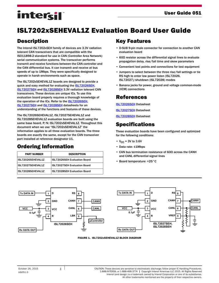
FIGURE 1. ISL7202xSEHEVAL1Z BLOCK DIAGRAM
October 26, 2015
UG051.0
1
CAUTION: These devices are sensitive to electrostatic discharge; follow proper IC Handling Procedures.
1-888-INTERSIL or 1-888-468-3774 | Copyright Intersil Americas LLC 2015. All Rights Reserved
Intersil (and design) is a trademark owned by Intersil Corporation or one of its subsidiaries.
All other trademarks mentioned are the property of their respective owners.
User Guide 051
Introduction
to easily interface with the IC to evaluate its functions, features
and performance.
The ISL72026SEHEVAL1Z, ISL72027SEHEVAL1Z and
ISL72028SEHEVAL1Z evaluation boards are exactly the same,
except for the CAN transceiver part installed at reference
designator U1.
This user guide will guide the user through the process of
configuring and using the evaluation board to evaluate the
ISL7202xSEH devices.
Functional Description
• The ISL72026SEHEVAL1Z has an ISL72026SEHF/PROTO IC
installed at U1. It will have a paper label indicating it is an
ISL72026SEHEVAL1Z board.
The ISL7202xSEHEVAL1Z evaluation board provides a simple
platform to demonstrate the features and evaluate the
performance of the ISL7202xSEH family of ICs. It provides easy
access to the pins of the ISL7202xSEH ICs and convenient
connectors/test points for connecting test equipment. The
schematic, bill of materials and top silkscreen for the board are
available on pages 9 through 11.
• The ISL72027SEHEVAL1Z has an ISL72027SEHF/PROTO IC
installed at U1. It will have a paper label indicating it is an
ISL72027SEHEVAL1Z board.
• The ISL72028SEHEVAL1Z has an ISL72028SEHF/PROTO IC
installed at U1. It will have a paper label indicating it is an
ISL72028SEHEVAL1Z board.
The ISL7202xSEHEVAL1Z boards are designed to provide a quick
and easy method for evaluating the ISL72026SEH,
ISL72027SEH and ISL72028SEH 3.3V radiation tolerant CAN
transceivers.
Table 1 shows the functional differences between the three part
types. Figure 1 shows the block diagrams/pinouts for the parts.
F
TABLE 1. TABLE OF DIFFERENCES BETWEEN THE PART TYPES
FEATURE
ISL72026SEH
ISL72027SEH
ISL72028SEH
Loopback
Yes
No
No
VREF Output
No
Yes
Yes
Listen Mode
Yes
Yes
No
Shutdown Mode
No
No
Yes
Supply Current in
Listen Mode
2mA
(maximum)
2mA
(maximum)
N/A
Supply Current in
Shutdown Mode
N/A
N/A
50µA
(maximum)
NOTE: N/A = Not Applicable
A picture of the evaluation board for ISL72028SEHEVAL1Z is
shown in Figure 6 on page 8. The ISL72028SEHF/PROTO 8 Ld
flatpack IC is soldered onto the evaluation board. It is located in
the upper center of the board and is designated as U1.
The Intersil ISL7202xSEH family of devices are 3.3V radiation
tolerant CAN transceivers that are compatible with the
ISO11898-2 standard for use in CAN (Controller Area Network)
serial communication systems. They were specifically designed
to operate in harsh environments such as space.
The transceiver performs transmit and receive functions between
the CAN controller and the CAN differential bus. It can transmit
and receive at bus speeds of up to 1Mbps. It is designed to
operate over a common-mode range of -7V to +12V with a
maximum of 120 nodes. The device is capable of withstanding
±20V on the CANH and CANL bus pins outside of ion beam and
±16V under ion beam.
The part has various configurations of operation. The evaluation
board contains standard jumpers, BNC connector, banana
connectors, cable connector and load resistors to allow the user
Submit Document Feedback
2
Figures 11 through 18 show performance data taken using the
ISL7202xSEHEVAL1Z evaluation board and basic lab equipment.
Table 1 shows the differences between the different parts in the
family.
The sections that follow will discuss using the evaluation board.
Basic Layout of Evaluation Board
The basic layout of the evaluation board is as follows: Refer to
Figure 10 on page 11 or the actual ISL7202xSEHEVAL1Z
evaluation board.
Located in the upper center of the board is the
IS7202xSEHF/PROTO transceiver IC (U1). The evaluation board
has a pin 1 dot, to show how the IC should be oriented onto the
evaluation board. The IC pin 1 indicator dot needs to be aligned
with the evaluation board pin 1 dot indicator. The board comes
with the IC soldered onto the board.
Power for the IC is located at the left side of the board through
banana jacks labeled VCC and GND. A DC voltage source of 3.3V
must be connected between VCC and GND to power the part. Test
points TP13 (VCC) and TP2 (GND) are available to measure the
VCC voltage to the part.
Access to the D input to the transceiver is at the BNC connector
labeled D at the upper right corner of the evaluation board. You
would connect the digital source of the CAN digital test pattern at
this connector.
Access to R output of the transceiver is at the test point labeled
TP4 located at the top center of the evaluation board. There is a
through-hole labeled R that could have a wire soldered to it, if you
want to feed the digital output into a CAN controller board.
Control of the RS pin is through jumpers J5, J6, J7 and J8 located
at middle left side of the evaluation board. Only one of these
jumper locations should have a jumper installed at any one time.
Putting the jumper at J5 will put the transceiver in the listen
mode for the ISL72026, ISL72027 parts and in the low power
shutdown mode for the ISL72028 part. Putting the jumper at J6
will put the transceiver driver in the slow speed mode, at J7 in the
medium speed mode, and at J6 in the fast speed mode. Note: J4
and R5 are not populated. They can be used to put a mechanical
potentiometer at the RS pin.
UG051.0
October 26, 2015
User Guide 051
Access to the differential pins (CANH and CANL) are through the
test points TP7 and TP8 or through the BNC connectors labeled
CANH and CANL (not populated) or through the D-SUB 9 pin male
connector J1, located at the bottom of the board. The J1
connector can be used to connect two evaluation boards
together, to evaluate the performance of two boards
communicating with each other over various length cables. The
CANH and CANL BNCs can be used to apply voltages to the
differential pins to evaluate the receiver of the transceiver.
The board comes populated with a 60Ω resistor (R10) installed
across the CANH and CANL lines. Many performance tests for the
transceiver such as propagation delay, rise time, fall time and
skew are done with a 60Ω resistor. In a normal CAN system the
bus is terminated at both ends with a 120Ω resistor, which gives
a differential loading of 60Ω.
See the board schematic (Figure 7 on page 9) for the reference
designators of the jumpers, resistors and connectors associated
with each I/O.
Power Supply
The ISL7202xSEH ICs require a DC power supply in the range of
3.0V to 3.6V for proper operation.
The power supply is connected at banana jacks VCC and GND.
The power supply should be capable of delivering 100mA of
current.
the transceiver remains active to allow for diagnostic testing of
the node. Installing a jumper at position 1 to 2 on jumper J9 of
the evaluation board will connect the LBK pin to VCC putting the
part in loopback state. Removing the jumper will put the part
back into normal operation. LBK pin of the transceiver has an
internal pull-down.
VREF PIN (ISL72027SEH AND ISL72028SEH)
The VREF pin (pin 5) of the ISL72027SEH and ISL72028SEH
parts outputs a voltage equal to VCC/2. This voltage is available
for applications that want to implement a split termination
configuration on the bus. See the application section titled “Split
Mode Termination” in the datasheets of the ISL72027SEH or
ISL72028SEH for more information. To implement a split
termination on the bus pins of the evaluation boardA capacitor
can be installed at C7, R11 and R12 can be populated with
resistors, and a jumper installed at position 2 and 3 of jumper J9.
Test Points
The board has various test points for ease of connecting probes
to make measurements. The test points available are described
in Table 2.
TABLE 2.
DESIGNATOR
DESCRIPTION
TP1
Ground test point
TP2
Ground test point
TP3
D input test point
TP4
R output test point
The ISL72027SEH and ISL72028SEH ICs have two logic control
input pins; the D (pin 1) and RS (pin 8).
TP5
LBK or VREF test point
TP6
RS pin test point
D PIN
TP7
CANH pin test point
The D pin is the digital input to the driver of the transceiver. A
digital bit pattern is applied at this pin. A logic 1 on the D pin puts
the CANH and CANL differential pins in the recessive state. A
logic 0 on the D pin puts the CANH and CANL differential pins in
the dominant state.
TP8
CANL pin test point
TP9
Ground test point
TP10
Not populated - VCM test point
TP11
Ground test point
TP12
Not populated - R output test point
TP13
VCC test point
Evaluation Board Logic Control
The ISL72026SEH IC has three logic control input pins; the D (pin
1), RS (pin 8) and LBK (pin 5).
The logic 1 VIH level is from 2.0V to 5.5V with a VCC supply
voltage of 3.0V to 3.6V. The logic 0 VIL level is from 0.8V to 0V.
RS PIN
The output driver rise and fall time has three distinct selections
that may be chosen by using a resistor from the RS pin to GND.
Connecting the RS pin directly to GND results in output switching
times that are the fastest, limited only by the drive capability of
the output stage. RS = 10kΩ provides for a typical slew rate of
8V/µs and RS = 50kΩ provides for a typical slew rate of 4V/µs.
Putting a high logic level to the RS pin places the transceiver in a
low current listen mode for the ISL72026SEH and ISL72027SEH
parts and a low current shutdown mode for the ISL72028SEH
part.
LBK PIN (ISL72026SEH)
When a high level is applied to the LBK pin, the device enters the
loopback state. The transceiver CANH and CANL pins are
disconnected from the bus. The driver and receiver circuitry of
Submit Document Feedback
3
UG051.0
October 26, 2015
User Guide 051
Board Component Definitions
DESIGNATOR
DESCRIPTION
U1
ISL7202xSEHF/PROTO flatpack IC
VCC
VCC power supply connection (3.3VDC)
GND
Ground connection
J1
9-pin male D-SUB connector (used to connect to another CAN evaluation board)
J4
Not populated - jumper on RS pin to connect mechanical potentiometer
J5
Jumper on RS pin to connect it to VCC (jumper installed at this location will put the transceiver in listen mode (ISL72026,
ISL72027) or shutdown mode (ISL72028)
J6
Jumper on RS pin to connect the RS pin to ground through a 50kΩ resistor (jumper installed at this location will put the
transceiver in slow speed mode).
J7
Jumper on RS pin to connect the RS pin to ground through a 10kΩ resistor (jumper installed at this location will put the
transceiver in medium speed mode).
J8
Jumper on RS pin to connect the RS pin to ground (jumper installed at this location will put the transceiver in high speed mode).
J9
Three pin jumper on the LBK pin (ISL72026) or VREF pin (ISL72027SEH, ISL72028SEH). Install jumper in upper position (1 to 2)
to put the ISL72026SEH device in loopback mode. Remove jumper for normal operation. Put jumper in lower position (2 to 3) to
connect CANH to CANL differential output pins for evaluation of split mode termination for ISL72027SEH and ISL72028SEH.
J10
Jumper, location is not populated. It needs to be populated if you are going to use BNC connector labeled CANH.
J11
Jumper, location is not populated. It needs to be populated if you are going to use BNC connector labeled CANL.
D
BNC connector. Provides access to the D pin of the transceiver.
CANH
BNC connector, location is not populated. Provides access to the CANH pin for special receiver testing and fault testing.
CANL
BNC connector, location is not populated. Provides access to the CANL pin for special receiver testing and fault testing.
FUNCTION
GENERATOR
0V to 3V
125kHz SQUARE WAVE
RS
TP6
D
TP1
R1
J6
R6
TP3
J7
R7
J8
R8
GND
50Ω
OSCILLOSCOPE
TP9
GND
J5
TP4
TP7
ISL72027SEH Eval1Z
R
U1
R15
CANH
CANL
C2
LOOP/SPLIT
CH1
CH2
CH3
CH4
TP3
D
TP7
CANH
TP8
CANL
TP4
R
R16
TP8
TP5
TP13
J1
R10
TP11
GND
TP9
GND
VCM
VCC
GND
+
Connect probes at the following test points
on the evaluation board.
-
DC POWER SUPPLY
+3.3V
FIGURE 2. BASIC EVALUATION TEST SETUP BLOCK DIAGRAM (MEASURING PROPAGATION DELAY, SKEW AND RISE/FALL TIME)
Submit Document Feedback
4
UG051.0
October 26, 2015
User Guide 051
Using the Board to Measure
Propagation Delay, Skew and
Rise/Fall Time
Refer to Figure 2 on page 4.
Lab Equipment
The equipment, external supplies and signal sources needed to
operate the board:
1. 3.3V DC power supply
2. Function/signal generator (HP 8112A pulse generator or
equivalent)
3. Four channel oscilloscope (Tektronix TDS5140 digital
oscilloscope or equivalent)
Initial Board Setup Procedure
1. Attach the main evaluation board to the DC power supply to
the banana jacks labeled VCC and GND as shown in Figure 2.
Positive terminal at VCC and negative terminal at GND. The
supply should be capable of delivering 3.0V to 3.6V and
100mA of current. Set the supply voltage to 3.3V.
5. Use the “Measure” menu of the oscilloscope to set up the
following four measurements:
a. LOW to HIGH propagation delay (tPLH) to measure the
time from the 50% point of the falling edge of CH1 (D
pin) to the 900mV point on the rising edge of the M1
trace (VDIFF).
b. HIGH to LOW propagation delay (tPHL) to measure the
time from the 50% point of the rising edge of CH1 (D pin)
to the 500mV point on the falling edge of M1 trace
(VDIFF).
c. Output rise time (tr) to measure the 10% to 90% time of
the rise edge of the M1 trace (VDIFF).
d. Output fall time (tf) to measure the 90% to 10% time of
the falling edge of the M1 trace (VDIFF).
6. Ensure that a jumper is installed at J8 (selects fast driver
edges by connecting the RS pin to ground) and no jumpers are
installed at J5, J6, J7 and J9.
7. Enable the function generator. The scope plots should look
like the ones shown in Figure 3 on page 6.
8. In fast speed mode (RS = 0V):
a. tPLH should be around 75ns and no greater than 150ns.
2. Configure the board for high speed mode by installing a
jumper at J8. No jumpers should be installed at J5, J6, J7 and
J9.
b. tPHL should be around 80ns and no greater than 155ns.
3. Connect the oscilloscope to the evaluation board as indicated
in Figure 2.
d. tfall should be around 25ns and no less than 10ns or
greater than 75ns.
c. trise should be around 55ns and no less than 20ns or
greater than 100ns.
a. Connect the Channel 1 probe to the D pin by connecting
the oscilloscope probe at TP3 on the evaluation board
and the probe ground at TP1.
9. Move the jumper from J8 to J7 (selects medium driver edges
by connecting the RS pin to ground through a 10kΩ resistor).
Note: No jumpers should be installed at J5, J6, J8 and J9.
b. Connect the Channel 2 probe to the CANH differential
pin by connecting the oscilloscope probe at TP7 on the
evaluation board and the probe ground at TP9.
10. The scope plot should look like the ones in Figure 4 on page 6.
c. Connect the Channel 3 probe to the CANL differential
pin by connecting the oscilloscope probe at TP8 on the
evaluation board and the probe ground at TP11.
d. Connect the Channel 4 probe to the R pin by connecting
the oscilloscope probe at TP4 on the evaluation board
and the probe ground at TP2.
4. Connect the function/signal generator at the BNC connector
labeled D on the evaluation board as shown in Figure 2. Set
the generator to output a 125kHz square wave, 0V to 3.3V
amplitude, 50% duty cycle with a trise = tfall ≤6ns. Disable the
generator output.
11. In medium speed mode (RS = 10kΩ):
a. tPLH should be around 520ns and no greater than
850ns.
b. tPHL should be around 460ns and no greater than
800ns.
c. tr should be around 400ns and no less than 200ns or
greater than 780ns.
d. tf should be around 300ns and no less than 175ns or
greater than 500ns.
12. Move the jumper from J7 to J6 (selects slow driver edges by
connecting the RS pin to ground through a 50kΩ resistor).
Note: No jumpers should be installed at J5, J7, J8 and J9.
5. Verify that a 60Ω resistor is installed at location R10 on the
evaluation board.
13. The scope plot should look like the ones in Figure 5 on page 7.
Calculating VDIFF and taking Measurements
a. tPLH should be around 850ns and no greater than
1400ns.
1. Set the oscilloscope to 2.0µs/division.
2. Set channel CH1 of the oscilloscope to 5V/division.
3. Set CH2, CH3 and CH4 of the oscilloscope to 2V/division
4. Using the math function of the oscilloscope, set the math 1
selection to measure CH2 - CH3 and display the M1 trace on
the oscilloscope screen.
M1 = CH2 - CH3 = VDIFF = CANH - CANL.
Submit Document Feedback
5
14. In slow speed mode (RS = 50kΩ):
b. tPHL should be around 725ns and no greater than
1300ns.
c. tr should be around 700ns and no less than 400ns or
greater than 1400ns.
d. tf should be around 650ns and no less than 300ns or
greater than 1000ns.
UG051.0
October 26, 2015
User Guide 051
ISL7202xSEHEVAL1Z Waveforms
FIGURE 3. OSCILLOSCOPE PLOT (FAST SPEED) WAVEFORMS AND MEASUREMENTS
FIGURE 4. OSCILLOSCOPE PLOT (MEDIUM SPEED) WAVEFORMS AND MEASUREMENTS
Submit Document Feedback
6
UG051.0
October 26, 2015
User Guide 051
ISL7202xSEHEVAL1Z Waveforms (Continued)
FIGURE 5. OSCILLOSCOPE PLOT (SLOW SPEED) WAVEFORMS AND MEASUREMENTS
Submit Document Feedback
7
UG051.0
October 26, 2015
User Guide 051
ISL7202xSEHEVAL1Z Evaluation Board
FIGURE 6. ISL72028SEHEVAL1Z EVALUATION BOARD
Submit Document Feedback
8
UG051.0
October 26, 2015
TP6
R5
J4
3
1
2
J10
1
VCC
J5
1
R6
J6
1
9
49.9K
R7
R1
R8
0
R15
0
2
C2
LOOP
TP1
330
R14
4
J1-6
6
CANL
5
J1-5
5
SPLIT
6
J1-4
7
J1-3
8
J1-2
9
J1-1
/SPLIT
0.1UF
R
ISL7202XSEH
GND
J1-7
CANH
C6
CANL
J1-8
3
7
330
VCC
J1-9
2
RS
R13
CANH
TP10
1
8
60.4
GND
60.4
R12
RS
R11
4
D
C5
R2
3
D-SUB CAN BUS
VCM
47PF
1
2
0.1UF
C1
J8
1
DNP
D
VCC
10UF
TP11
2
U1
R
GND
1000PF
DUT
R16
TP2
0
TP12
C4
1000PF
TP5
TP8
J11
R
1
1
2
1
2
0
2
4 5
3
C7
J9
0.047UF
C8
15PF
VCC
TP9
CANL
R17
3
TP4
DRAWN BY:
FIGURE 7. SCHEMATIC
DATE:
ALAN ERZINGER
ENGINEER:
04/28/2015
ALLAN ROBINSON
DATE:
User Guide 051
3.0V-3.6V
C3
2
0
TP13
VCC
2
60.4
1
3 2
5
1
4 5
10K
4
D
TP3
1
2
0
R10
D
J7
CANH
R9
2
TP7
3
100K
1
2
Submit Document Feedback
ISL7202xSEHEVAL1Z Circuit Schematic
UG051.0
October 26, 2015
User Guide 051
ISL7202XSEHEVAL1Z Bill of Materials
QTY UNITS
REFERENCE
DESIGNATOR
DESCRIPTION
SEE LABEL - RENAME PWB-PCB, ISL7202XEVAL1Z, Rev A, ROHS
BOARD
MANUFACTURER
PART NUMBER
MFR
1
ea.
1
ea.
C2
CAP, SMD, 0805, 0.1µF, 50V, 10%, X7R, ROHS
KEMET
C0805C104K5RACTU
1
ea.
C1
CAP, SMD, 0805, 10µF, 25V, 10%, X5R, ROHS
TDK
C2012X5R1E106K
1
ea.
D
CONN - BNC, RECEPTACLE, TH, 4 POST, 50Ω, GOLDCONTACT, ROHS
AMPHENOL
31-5329-52RFX
1
ea.
TP13
CONN - MINI TEST PT, VERTICAL, RED, ROHS
KEYSTONE
5000
4
ea.
TP1, TP2, TP9, TP11 CONN - MINI TEST PT, VERTICAL, BLK, ROHS
KEYSTONE
5001
2
ea.
KEYSTONE
5002
4
ea.
KEYSTONE
5004
1
ea.
J1
3
ea.
GND, VCC, VCM
1
ea.
1
TP7, TP8
CONN-MINI TEST PT, VERTICAL, WHITE, ROHS
TP3, TP4, TP5, TP6 CONN-MINI TEST PT, VERTICAL, YEL, ROHS
IMAGINEERING ISL7202XEVAL1ZREVAPCB
INC
9 PIN MALE RIGHT ANGLE D-SUB CONNECTOR
5788792-1
TE
CONNECTIVITY
/ AMP
CONN - JACK, MINI BANANA, 0.175 PLUG, NICKEL/BRASS, ROHS
KEYSTONE
575-4
U1
CAN BUS PART, 8P, FLAT-PACK, GOLD, ROHS
INTERSIL
ISL7202XSEHF/PROTO
ea.
J9
CONN - HEADER, 1X3, BREAKAWY 1X36, 2.54mm, ROHS
BERG/FCI
68000-236HLF
4
ea.
J5, J6, J7, J8
CONN - HEADER, 1X2, RETENTIVE, 2.54mm, 0.230X0.120, ROHS
BERG/FCI
69190-202HLF
0
ea.
R2, R9, R11, R12,
R13, R14, R17
RESISTOR, SMD, 0805, DNP, TF, ROHS
-
-
4
ea.
R1, R8, R15, R16
RES, SMD, 0805, 0Ω, 1/8W, TF, ROHS
YAGEO
RC0805JR-070RL
1
ea.
R7
RES, SMD, 0805, 10kΩ, 1/8W, 1%, TF, ROHS
VENKEL
CR0805-8W-1002FT
(PbFREE)
1
ea.
R6
RES, SMD, 0805, 49.9kΩ, 1/8W, 1%, TF, ROHS
PANASONIC
ERJ-6ENF4992V
1
ea.
R10
RES, SMD, 0805, 60.4Ω, 1/8W, 1%, TF, ROHS
PANASONIC
ERJ-6ENF60R4V
4
ea.
Four Corners
SCREW, 4-40X1/4in, PAN, SS, PHILLIPS
-
-
4
ea.
Four Corners
STANDOFF, 4-40X3/4in, F/F, HEX, ALUMINUM, ROHS
KEYSTONE
2204 (.250 OD)
1
ea.
Place assy in bag
BAG, STATIC, 6X8, ZIP LOC, ROHS
ULINE
S-2262
0
ea.
TP10, TP12
CONN-MINI TEST POINT, VERTICAL, ROHS
KEYSTONE
5004
0
ea.
0
ea.
J4, J10, J11
DO NOT POPULATE OR PURCHASE
0
ea.
R5
DO NOT POPULATE OR PURCHASE
0
ea.
CANH, CANL
DO NOT POPULATE OR PURCHASE
1
ea.
INTERSIL
LABEL-DATE CODE
C3, C4, C5, C6, C7, DO NOT POPULATE OR PURCHASE
C8
AFFIX TO BACK OF LABEL-DATE CODE_LINE 1: YRWK/REV#, LINE 2: BOM NAME
PCB
Submit Document Feedback
10
UG051.0
October 26, 2015
User Guide 051
Board Layout
FIGURE 8. TOP LAYER
FIGURE 9. BOTTOM LAYER
FIGURE 10. TOP LAYER SILK SCREEN
Submit Document Feedback
11
UG051.0
October 26, 2015
User Guide 051
Typical Performance Curves
Unless noted: VCC = 3.3V, D = 125kHz, Square Wave, 0 to VCC, 50% Duty Cycle,
R
0
3
RS = GND, RD = 60Ω
2
1
CANH - CANL
0
4
R
0
3
RS = 10kΩ, RD = 60Ω
2
CANH - CANL
1
0
TIME (1µs/DIV)
FIGURE 12. MEDIUM DRIVER AND RECEIVER WAVEFORMS
4
D
0
4
RS = GND, RD = 60Ω
3
H TO L, VCC = 3V
100
L TO H, VCC = 3V
80
TIME (ns)
0
R
120
DRIVER INPUT (V)
RECEIVER OUTPUT (V)
0
TIME (1µs/DIV)
FIGURE 11. FAST DRIVER AND RECEIVER WAVEFORMS
DRIVER OUTPUT (V)
4
D
DRIVER INPUT (V)
4
RECEIVER OUTPUT (V)
0
DRIVER INPUT (V)
4
D
DRIVER OUTPUT (V)
DRIVER OUTPUT (V)
RECEIVER OUTPUT (V)
tr = tf ≤6ns, TA = +25°C
L TO H, VCC = 3.6V
60
H TO L, VCC = 3.6V
40
RS = 50kΩ, RD = 60Ω
2
CANH - CANL
20
1
SKEW, VCC = 3.6V
0
-55
0
TIME (1µs/DIV)
FIGURE 13. SLOW DRIVER AND RECEIVER WAVEFORMS
Submit Document Feedback
12
-35
-15
SKEW, VCC = 3V
5
25
45
65
85
105
125
TEMPERATURE (°C)
FIGURE 14. TRANSMITTER PROPAGATION DELAY AND SKEW vs
TEMPERATURE AT FAST SPEED
UG051.0
October 26, 2015
User Guide 051
Typical Performance Curves
Unless noted: VCC = 3.3V, D = 125kHz, Square Wave, 0 to VCC, 50% Duty Cycle,
tr = tf ≤6ns, TA = +25°C (Continued)
800
1200
RS = 10kΩ, RD = 60Ω
700
L TO H, VCC = 3V
RS = 10kΩ, RD = 60Ω
L TO H, VCC = 3V
1000
600
TIME (ns)
L TO H, VCC = 3.6V
H TO L, VCC = 3.6V
400
H TO L, VCC = 3V
TIME (ns)
800
500
300
L TO H, VCC = 3.6V
H TO L, VCC = 3.6V
600
H TO L, VCC = 3V
400
200
SKEW, VCC = 3V
SKEW, VCC = 3V
200
100
0
-55
SKEW, VCC = 3.6V
0
-55
-35
-15
5
SKEW, VCC = 3.6V
-35
-15
5
25
45
65
TEMPERATURE (°C)
85
105
125
FIGURE 15. TRANSMITTER PROPAGATION DELAY AND SKEW vs
TEMPERATURE AT MEDIUM SPEED
25
45
65
TEMPERATURE (°C)
85
105
125
FIGURE 16. TRANSMITTER PROPAGATION DELAY AND SKEW vs
TEMPERATURE AT SLOW SPEED
60
600
RS = GND, RD = 60Ω
RS = 10kΩ, RD = 60Ω
55
500
RISE, VCC = 3V
45
RISE, VCC = 3.6V
40
35
30
300
FALL, VCC = 3V
FALL, VCC = 3.6V
200
FALL, VCC = 3V
-35
-15
100
FALL, VCC = 3.6V
25
20
-55
RISE, VCC = 3.6V
400
RISE, VCC = 3V
TIME (ns)
TIME (ns)
50
5
25
45
65
85
105
125
TEMPERATURE (°C)
FIGURE 17. TRANSMITTER RISE AND FALL TIMES vs TEMPERATURE
AT FAST SPEED
0
-55
-35
-15
5
25
45
65
TEMPERATURE (°C)
85
105
125
FIGURE 18. TRANSMITTER RISE AND FALL TIMES vs TEMPERATURE
AT MEDIUM SPEED
Intersil Corporation reserves the right to make changes in circuit design, software and/or specifications at any time without notice. Accordingly, the reader is
cautioned to verify that the document is current before proceeding.
For information regarding Intersil Corporation and its products, see www.intersil.com
Submit Document Feedback
13
UG051.0
October 26, 2015
