Method of Selection of dv/dt for EMI Current Ringing Attenuation
advertisement
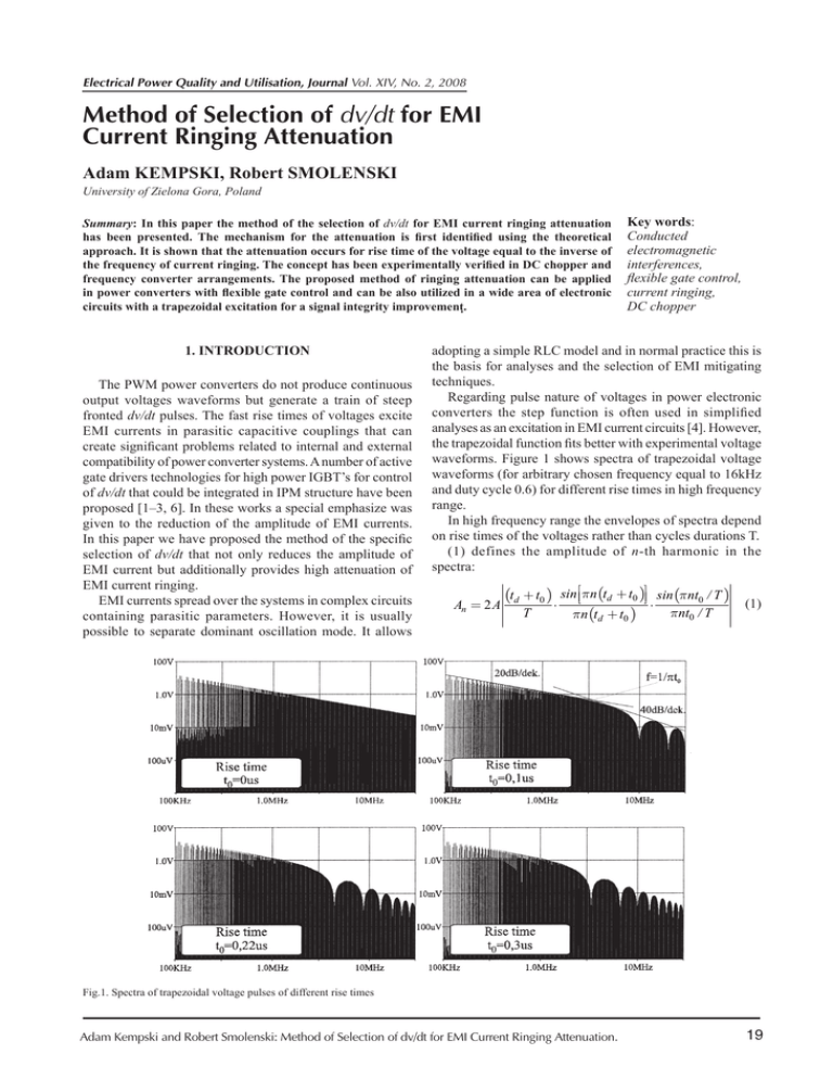
Electrical Power Quality and Utilisation, Journal Vol. XIV, No. 2, 2008 Method of Selection of dv/dt for EMI Current Ringing Attenuation Adam Kempski, Robert Smolenski University of Zielona Gora, Poland Summary: In this paper the method of the selection of dv/dt for EMI current ringing attenuation has been presented. The mechanism for the attenuation is first identified using the theoretical approach. It is shown that the attenuation occurs for rise time of the voltage equal to the inverse of the frequency of current ringing. The concept has been experimentally verified in DC chopper and frequency converter arrangements. The proposed method of ringing attenuation can be applied in power converters with flexible gate control and can be also utilized in a wide area of electronic circuits with a trapezoidal excitation for a signal integrity improvement. 1. Introduction The PWM power converters do not produce continuous output voltages waveforms but generate a train of steep fronted dv/dt pulses. The fast rise times of voltages excite EMI currents in parasitic capacitive couplings that can create significant problems related to internal and external compatibility of power converter systems. A number of active gate drivers technologies for high power IGBT’s for control of dv/dt that could be integrated in IPM structure have been proposed [1–3, 6]. In these works a special emphasize was given to the reduction of the amplitude of EMI currents. In this paper we have proposed the method of the specific selection of dv/dt that not only reduces the amplitude of EMI current but additionally provides high attenuation of EMI current ringing. EMI currents spread over the systems in complex circuits containing parasitic parameters. However, it is usually possible to separate dominant oscillation mode. It allows Key words: Conducted electromagnetic interferences, flexible gate control, current ringing, DC chopper adopting a simple RLC model and in normal practice this is the basis for analyses and the selection of EMI mitigating techniques. Regarding pulse nature of voltages in power electronic converters the step function is often used in simplified analyses as an excitation in EMI current circuits [4]. However, the trapezoidal function fits better with experimental voltage waveforms. Figure 1 shows spectra of trapezoidal voltage waveforms (for arbitrary chosen frequency equal to 16kHz and duty cycle 0.6) for different rise times in high frequency range. In high frequency range the envelopes of spectra depend on rise times of the voltages rather than cycles durations T. (1) defines the amplitude of n-th harmonic in the spectra: An = 2 A (td + t0 ) sin πn (td + t0 ) sin (πnt0 / T ) (1) ⋅ ⋅ T πnt0 / T πn (td + t0 ) Fig.1. Spectra of trapezoidal voltage pulses of different rise times Adam Kempski and Robert Smolenski: Method of Selection of dv/dt for EMI Current Ringing Attenuation. 19 where: T — cycle of trapezoidal pulses, td ­— impulse width, t0 ­— rise time of impulse. Although the frequency of the oscillation in circuit with trapezoidal excitation depends on parameters of passive elements, a resulting shape and a maximum value of the current are strongly influenced by rise and fall time of the voltage slopes. The control of dv/dt is one of the known mitigation technique, however, benefits of this simple method are counterbalanced by the increasing of switching losses in hard-switched power converters. The ringing phenomena can exacerbate the problems of EMI, overvoltages and signal integrity in systems containing power electronic converters. Additionally, the ringing transient can not fully decay before the application of the next pulse that can cause overvoltages higher then in a case of single pulse (double pulsing). The main of the objectives of the paper is to propose the way in which the rise time of the voltage could be chosen regarding frequency of resonant circuit. For convenience of analyses leading edge of a trapezoidal signal can be split into linear excitations, as shown in Figure 2. Time varying voltage u(t) can be expressed as the sum of the linear function f1(t) = (DU / t0) t and the same function with opposite sign shifted by time t0, as follows: u (t )= ∆U t ⋅ 1(t )− ∆U (t − t0 )⋅ 1(t − t0 ) t0 t0 (2) Laplace transform of the (2) using shift theorem can be expressed as: F (s )= ∆U 12 − ∆U 12 e−st0 = ∆U 12 1− e−st0 (3) t0 s t0 s t0 s ) The current transform in second-order series RLC circuit can be written as: s I (s )= U 12 1 1− e st0 = t0 s L (s − α)2 + ω 2 0 ( ) st0 1 1 1 = U 1 1 − e t0 L s (s − α)2 + ω 2 s (s − α)2 + ω 2 0 0 (4) Using inverse Laplace transform the waveform of the current in this circuit is given by: K 1(t )− Ae−αt sin (ω t + β )1(t )+ 0 − α t −t0 ) ( U 1 i (t )= K t t Ae − − − 1 ( ) 0 t0 L sin (ω0 (t − t0 )+ β )1(t − t0 ) 20 where: 2 ω02 = ωn2 − α 2 = 1 − R 2 LC 4 L R, L, C — resulting resistance, inductance and capacitance of the circuit, a = R / 2L — damping factor, A= 1 ω0 2. Theoretical analysis ( Fig. 2. Excitation used in theoretical analysis (5) 1 α 2 + ω02 K= 1 α 2 + ω02 β = arctg ω0 α Figure 3 shows current responses of the series RLC circuit on excitation shown in Figure 2 with different rise time t0. For the specific rise time of the voltage (t0=1/f where f is resonant frequency of the circuit) it has been observed ringing attenuation. The spectra of presented currents are shown in Figure 4. Figure 5 shows three-dimensional graphs of the mathematical relations between the amplitudes of currents (first peak of current in Fig. 4a, and amplitude of first oscillation after the time t0 in Fig.4b), the rise time of the voltage and the pulsation of the resonant circuit. The local minima in the graph define circumstances in which a ringing is highly attenuated. 3. Experimental results The theoretical results have been verified in the experimental arrangement with a DC chopper shown in Figure 6. Figure 7 shows the waveforms of collector-emitter voltages UCE with different rise times t0 corresponding to values from Fig. 1 selected for theoretical analysis. The rise and fall times have been controlled by means of gate resistors RG1 and RG2. The envelopes of the spectra of collector-emitter voltages UCE for different rise times have been shown in Figure 8. These envelopes have been obtained using EMI receiver with intermediate frequency bandwidth (IF BW) equal to 120 kHz and average detector. The shape of the spectra envelopes of UCE show consistence with theoretical voltage spectra showed in Figure 1, in spite of the fact that experimental waveforms of collector-emitter voltage look smoother than the theoretical ones (because of the IF BW filters). Power Quality and Utilization, Journal • Vol. XIV, No 2, 2008 Fig.3. EMI currents for different rise times. Fig. 4. Spectra of EMI currents for different rise times Application capabilities of the proposed method have been proven for the attenuation of the CM current ringing, in a DC chopper arrangement of resonant frequency determined by the parasitic parameters of the CM current that flow through parasitic capacitive couplings as the result of high dv/dt excitation of the circuit, Figure 6. Figure 8, shows the spectra of CM currents for different rise times of UCE voltage. The theoretical analyses have shown that the attenuation of current ringing is connected with a lack of harmonics in voltage spectrum related to resonant frequency f0 of CM current path. This frequency is approximately equal to 3.6 MHz, Figure 9. The attenuation occurs for the rise time t0=1/f0=0.28 µs and it is visible as a lack of the peak of the spectrum in this case. Fig. 10 shows the influence of rise time of the UCE voltage on the CM current waveforms. The attenuation is provided indeed for the rise time of UCE equal to 0.28µs. Adam Kempski and Robert Smolenski: Method of Selection of dv/dt for EMI Current Ringing Attenuation. 21 Fig. 7. Collector-emitter voltages of different rise times Fig. 5. 3D graphs of currents amplitudes, rise time of voltage and pulsation Fig. 8. Envelopes of the spectra of collector-emitter voltages Fig. 6. Experimental arrangement Figure 5 and (5) show that the similar effect of attenuation could be achieved by changing of the resonant frequency of the current circuit. As an exemplification there is presented the experimental results obtained in a system consist of a frequency converter and open-ended long cable. Additional issue in such system is that it is necessary to consider circuits of distributed parameters. Figure 11 shows common mode currents in the PE wire of the open ended cable of different length and Figure 12 shows spectra of these currents. Generally, the level of common mode EMI in open-ended cable is proportional to the length of the cable (6dB for 22 Fig. 9. Spectra of the CM currents for different rise time of collector-emitter voltages doubled length of the cable) because of evenly distributed parasitic parameters along the cable. However, each line of specific length has resonant frequency, which results from the length of the line and the velocity of the traveling wave [5]. A current in a lossy line with very high dv/dt excitation has approximately damped oscillatory waveform that is represented as a peak in the spectrum. Using traveling wave theory it can be shown [7] that the ringing attenuation occurs when rise time is equal to the four times the time that is required for the wave front to travel along the length of the Power Quality and Utilization, Journal • Vol. XIV, No 2, 2008 Fig. 10. Collector-emitter voltages and EMI currents for different voltage rise times Fig. 11. Common mode current in drive with different cable length line. In the Fiure 11 such phenomenon occurs for the specific cable length equal to 8m and in this case the spectrum has no resonant peak. 4. Conclusion In the technical literature, a number of active gate drives technologies for flexibly controlling the output voltage dv/ dt of power devices during hard switching events have been proposed. These techniques allow EMI reduction by means of the control of rise and fall times of collectoremitter voltages. However, a compromise is needed between lowering EMI and increasing switching losses that limits a freedom of the selection appropriate dv/dt. The main objective of this paper is to propose the method of the selection of dv/dt in the range of this freedom that not only reduces overshot amplitudes but additionally assures high attenuation of EMI current ringing. The proposed method of the selection of dv/dt (or resonant frequency of the circuit) has a potential to become a way for achieving of Fig.12. Spectra of CM current in drive with different cable length desired shape of EMI spectrum of the systems containing power converters in the specific frequency range. The proposed method of ringing attenuation can be also utilized in a wide area of electronic circuits with a trapezoidal excitation for a signal integrity improvement. Adam Kempski and Robert Smolenski: Method of Selection of dv/dt for EMI Current Ringing Attenuation. 23 References 1.P a r k S . , J a h n s T. M .: Flexible dv/dt and di/dt control method for insulated gate power switches. IEEE Trans. on Industry Applications, 2003, Vol. 39, No. 3, pp. 657–664. 2.J o h n V. , S u h B - S . , L i p o T. A .: High performance active gate drive for high power IGBTs. IEEE Trans. on Industry Applications, 1999, Vol. 35, No. 5, pp.1108–1117. 3.G r e s e r C . , H o p f e r P. : Gate Controled dv/dt and di/dt limitation in High Power IGBT Converters. EPE Journal, 1996, Vol. 5. 4.O g a s a w a r a S . , A k a g i H . : Modeling and damping of highfrequency leakage currents in PWM inverter-fed ac motor drive systems. IEEE Trans. Ind. Appl., 1996, vol. 32, no. 5, pp. 1105– 1114. 5.M a g n u s s o n P. C . , A l e x a n d e r G . C . , T r i p a t h i V. K . , We i s s h a a r A . : Transmission lines and wave propagation. CRC Press. 6.K a t o h S . , U e d a S . , S a k a i H . , I s h i d a T. , E g u c h i Y. : Active-gate-control for snubberless IGBTs connected in series. Power Electronics Specialists Conference 2002, Vol. 2, June 2002, pp.609–613. 7.K e m p s k i A , S m o l e n s k i R . , S t r z e l e c k i R . : Common mode current paths and their modeling in PWM in-verter-fed drives. Power Electronics Specialists Conference, Vol. 3, pp.1551–1556, Cairns, Australia. Adam Kempski was born in 1953 in Kepno, Poland. He received the M.Sc. and Ph.D. degrees in electrical engineering from Technical University of Wroclaw and post-doctoral degree from University of Zielona Gora. At present he is a Researcher and Head of Division of Institute of AT Electrical Engineering at University of Zielona Gora. His field of interest is Electromagnetic Compatibility in Power Electronics. Address: University of Zielona Gora, Institute of Electrical Engineering, ul. Podgorna 50, 65-246 Zielona Gora, e-mail: A.Kempski@iee.uz.zgora.pl phone/fax: +48 68 328 25 38/+48 68 324 72 93 Robert Smolenski was born in 1973 in Krosno Odrzanskie, Poland. He received the M.Sc. and Ph.D. degree in electrical engineering from Technical University of Zielona Gora. At present he is a Researcher and Deputy Head of Institute at Electrical Engineering in University of Zielona Gora. His field of interest is Electromagnetic Compatibility in Power Electronics. Address: University of Zielona Gora, Institute of Electrical Engineering, ul. Podgorna 50, 65-246 Zielona Gora, e-mail: R.Smolenski@iee.uz.zgora phone/fax: +48 68 328 25 38/+48 68 324 72 93 24 Power Quality and Utilization, Journal • Vol. XIV, No 2, 2008
