MLX74190
Two-Fold High Power LF Initiator
With integrated Immobilizer
Features and Benefits
Application Examples
2 High power independent drivers (2.5Apeak in
square and 1Apeak in sine mode)
Full bridge drive capabilities
Built-in protection features (antenna fault detection,
over current and T°) for guaranteed safe operation
in all conditions
Easy-to-use through SPI interface
Built-in ASK and FSK immobilizers
Passive Start system
TPMS Initiator
LF door opener
Active RFID initiator
Ordering Information
Part Code
Temperature Code
Package Code
MLX74190
R (-40°C to 105°C)
PF (Lead free TQFP 7x7 48 leads)
Option
Code
ABA-000
Packing Form
Code
RE
This document is a Product Preview, to get access to the full datasheet and related documentations, please directly
contact Melexis at sales_europe@melexis.com or sales_usa@melexis.com.
Description
The MLX74190 low-frequency (LF) initiator IC consists in two high power LF drivers and built-in immobilizers
(IMMO).
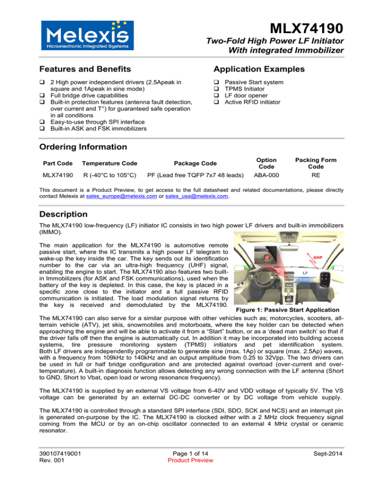
The main application for the MLX74190 is automotive remote
passive start, where the IC transmits a high power LF telegram to
wake-up the key inside the car. The key sends out its identification
number to the car via an ultra-high frequency (UHF) signal,
enabling the engine to start. The MLX74190 also features two builtin Immobilizers (for ASK and FSK communications), used when the
battery of the key is depleted. In this case, the key is placed in a
specific zone close to the initiator and a full passive RFID
communication is initiated. The load modulation signal returns by
the key is received and demodulated by the MLX74190.
Figure 1: Passive Start Application
The MLX74190 can also serve for a similar purpose with other vehicles such as; motorcycles, scooters, allterrain vehicle (ATV), jet skis, snowmobiles and motorboats, where the key holder can be detected when
approaching the engine and will be able to activate it from a “Start” button, or as a ‘dead man switch’ so that if
the driver falls off then the engine is automatically cut. In addition it may be incorporated into building access
systems, tire pressure monitoring system (TPMS) initiators and pet identification system.
Both LF drivers are independently programmable to generate sine (max. 1Ap) or square (max. 2.5Ap) waves,
with a frequency from 109kHz to 140kHz and an output amplitude from 0.25 to 32Vpp. The two drivers can
be used in full or half bridge configuration and are protected against overload (over-current and overtemperature). A built-in diagnosis function allows detecting any wrong connection with the LF antenna (Short
to GND, Short to Vbat, open load or wrong resonance frequency).
The MLX74190 is supplied by an external VS voltage from 6-40V and VDD voltage of typically 5V. The VS
voltage can be generated by an external DC-DC converter or by DC voltage from vehicle supply.
The MLX74190 is controlled through a standard SPI interface (SDI, SDO, SCK and NCS) and an interrupt pin
is generated on-purpose by the IC. The MLX74190 is clocked either with a 2 MHz clock frequency signal
coming from the MCU or by an on-chip oscillator connected to an external 4 MHz crystal or ceramic
resonator.
390107419001
Rev. 001
Page 1 of 14
Product Preview
Sept-2014
MLX74190
Two-Fold High Power LF Initiator
With integrated Immobilizer
Table of Contents
1 Absolute Maximum Ratings..............................................................................................................................3
2 Range of Functionality......................................................................................................................................3
1 Pin out description ............................................................................................................................................4
2 High Level Block Diagram ................................................................................................................................6
3 Operating Modes ..............................................................................................................................................7
3.1 Sleep Mode ................................................................................................................................................7
3.2 Standby Mode ............................................................................................................................................7
3.3 Transmission Mode ...................................................................................................................................7
3.4 Diagnosis Mode .........................................................................................................................................7
4 Device Description ...........................................................................................................................................8
4.1 Power supplies, internal regulation and references ..................................................................................8
4.2 System clock ..............................................................................................................................................8
4.3 Low Frequency Generation .......................................................................................................................8
4.4 Sine wave generation ................................................................................................................................8
4.5 Square wave generation ............................................................................................................................8
4.6 Modulator ...................................................................................................................................................8
4.7 Immobilizer ASK ........................................................................................................................................8
4.8 Immobilizer FSK ........................................................................................................................................9
4.9 Digital SPI Interface ...................................................................................................................................9
4.10 SPI Commands ........................................................................................................................................9
4.11 Failure Flags ............................................................................................................................................9
4.12 Antenna diagnosis ...................................................................................................................................9
4.13 Current Measurement ..............................................................................................................................9
5 Application Information ...................................................................................................................................10
1 Package and marking information ..................................................................................................................11
1.1 Package data TQFP eP 48L (7x7, 48 leads) ...........................................................................................11
1.2 Marking instruction ...................................................................................................................................12
2 Standard information regarding manufacturability of Melexis products with different soldering processes ..13
3 Disclaimer .......................................................................................................................................................14
4 Contact Information ........................................................................................................................................14
390107419001
Rev. 001
Page 2 of 14
Product Preview
Sept-2014
MLX74190
Two-Fold High Power LF Initiator
With integrated Immobilizer
1 Absolute Maximum Ratings
Parameter
Symbol
Driver Supply Voltage
5V Supply
Storage Temperature Range
Junction Temperature
Static thermal resistance from
Junction to Ambient
Min
Max
Units
VS
VDD
TS
-55
45
7
150
V
V
C
Tj
-40
165
C
28
K/W
Rthja
Comment
ESD Sensitivity (HBM global pins)
VESDglobal
+/-3
kV
OUT1, OUT2, VS,
ASK_RXi, FSK_RXi
ESD Sensitivity (HBM local pins)
VESDlocal
+/-2
kV
All other pins
ESD Sensitivity (CDM)
VCDM_sens (HBM
+/-500
Global pins)
Table 1: Absolute maximum ratings
V
Exceeding the absolute maximum ratings may cause permanent damage. Exposure to absolute-maximumrated conditions for extended periods may affect device reliability.
2 Range of Functionality
Parameter
Symbol
Min Value
Typical
Max Value
Units
5V Supply
VDD
4.5
5
5.5
V
Driver Supply Voltage – operating
VS
6
-
40
V
Input voltage range on pins: NCS,
SCLK, SDI, WUP, CLK_IN and
REMOTE_DATA_IN, OSC
Vin_dig
-0.5
VDD
5.5
V
TA
-40
-
105
C
Operating Temperature Range
Table 2: Range of functionality
Note:
Every electrical parameter specified in this document, except if specifically indicated, is valid in the complete
temperature range: -40 / 105C.
390107419001
Rev. 001
Page 3 of 14
Product Preview
Sept-2014
MLX74190
Two-Fold High Power LF Initiator
With integrated Immobilizer
1 Pin out description
Pin №
Name
Type
Function
1
FSK_RX2
Analog
FSK Immobilizer input pin 2
2
FSK_FB2
Analog
FSK Immobilizer feedback loop 2
3
IP_SENSE
Analog
Current Measurement Output Voltage
4
RBIAS
Analog
Reference Resistor connection for trimming the current reference
5
EXT_CLK
Digital
External clock used in combination with CLK_IN to connect an external resonator
6
CLK_IN
Digital
Input clock coming from MCU or connected to external resonator
7
OSC
Analog
125KHz clock input/output
8
OUT1
Analog
Antenna connection (driver output 1)
9
GND
Ground
Power ground for driver outputs
10
VS
Supply
Supply for driver outputs
11
OUT2
Analog
Antenna connection (driver output 2)
12
CLK_OUT
Digital
2MHz clock output
13
WUP
Digital
Wake up pin
15
SCLK
Digital
Serial clock for SPI
16
NCS
Digital
Not chip select for SPI
17
SDO
Digital
Slave data output for SPI
18
SDI
Digital
Slave data input for SPI
19
IRQ
Digital
Interrupt signal output
20
D_OUT
Digital
Immobilizer data / Digital modulation output signal
21
RDI
Digital
Input signal for direct LF modulation (RDI = Remote_Data_In)
22
VDDA_CAP
Supply
Analog internal regulator decoupling cap.
23
ASK_RX1
Analog
ASK Immobilizer input 1
24
ASK_RX2
Analog
ASK Immobilizer input 2
25
AGND
Ground
Analog ground
36
VDD
Supply
5V supply
38
DGND
Ground
Digital ground
41
VDDD_CAP
Supply
Digital internal regulator decoupling capacitor
47
FSK_RX1
Analog
FSK Immobilizer input pin 1
48
FSK_FB1
Analog
FSK Immobilizer feedback loop 1
14, 46
26,27,28,29,30,
31,32, 33, 34,
35, 37,39, 40,
42, 43, 44, 45
Reserved
NA
Must be externally connected to ground
NC
NA
Not connected
EXP
EXP
Ground
Exposed PAD, to be connected to ground
Table 3: Pin out description
390107419001
Rev. 001
Page 4 of 14
Product Preview
Sept-2014
MLX74190
n.c.
n.c.
DGND
n.c.
40
39
38
37
41
n.c.
44
n.c.
n.c.
45
n.c.
VDDD_CAP
n.c.
46
42
FSK_RX1
47
43
FSK_FB1
48
Two-Fold High Power LF Initiator
With integrated Immobilizer
1
36
VDD
FSK_FB2
2
35
n.c.
IP_SENSE
3
34
n.c.
RBIAS
4
33
n.c.
EXT_CLK
5
32
n.c.
CLK_IN
6
31
n.c.
30
n.c.
29
n.c.
23
24
ASK_RX2
21
RDI
22
20
D_OUT
ASK_RX1
19
VDDA_CAP
18
SDI
WUP
IRQ
12
17
CLK_OUT
16
11
NCS
OUT2
SDO
10
13
VS
15
GND
9
14
8
n.c.
OUT1
SCLK
OSC
7
MLX
74190
zzzzzzzzz
yyww
FSK_RX2
28
n.c.
27
n.c.
26
n.c.
25
AGND
Table 4: Top view of the package TQFP48
390107419001
Rev. 001
Page 5 of 14
Product Preview
Sept-2014
MLX74190
Two-Fold High Power LF Initiator
With integrated Immobilizer
2 High Level Block Diagram
MLX74190
FSK/ASK Immobilizers
FSK_En
FSK_InSel
FSK_RX1
Bias current references,
automatic trimming
Pre-regulator
+ High-accuracy Band-gap
VDD
Data
slicer
FSK_DataOut
RBIAS
FSK_FB1
Band-pass filter
FSK_RX2
Vdda
FSK_FB2
VDDA_CAP
AGND
ASK_En
Porb
POR
Vddd
Digital
Regulator
VDDD_CAP
Analog
Regulator
ASK_RX1
Power supplies, internal
regulation and references
ASK_AdcOut
DGND
ASK_ADCstart
ASK_ADCready
Digital_modulation
ASK_RX2
ASK_InSel
ASK_InRg[1:0]
Output of line-coding state machine
RSSI
Remote_DATA_IN
REMOTE_DATA_IN
Input stage
filter
ADC
Immo Demod Out
Start/Stop
Digital
D_OUT
Digital Modulation Signal
IMMO-FSK
WUP
Test & NAND
Tree
SCLK
SDI
SDO
NCS
IRQ
Mod_In
Controller
Transmission
Immobilizer
SPI
Registers
VS
PGA
Counter
Voltage
references
Diagnosis
FSM
I_out1
Modul+phase
Sinus
DAC
GND
Phase
Modulator
Signal generator
VS
FSK_DataOut
Porb
PGA
Voltage
references
ASK_AdcOut
ASK / FSK immobilizer
OUT1
Driver
Filter
Immo Demod Out
Modul+phase
Sinus
DAC
OUT2
Driver
Filter
I_out2
Phase
Modulator
GND
PGA_In_Square
Duty cycle
controller
LF transmission chain
Clk_32MHz
Control blocks
System clock
PLL x16
Master/slave
VS
Monitoring
VS_uv
VDD
VDD
Monitoring
VDD_uv
Clk_Osc
Temperature
Monitoring
Clk_2MHz
Clock
divider
CLK_IN
EXT_CLK
CLK_OUT
Diagnosis Flag
VS
OSC
Diagnosis
OverC flag
OVT
TPW
RBIAS
OverCurrent
protection
AC-current peak
detector
I_out1
I_out2
I_out1
I_out2
IP_SENSE
RBIAS
Figure 2: MLX74190 high level block diagram
390107419001
Rev. 001
Page 6 of 14
Product Preview
Sept-2014
MLX74190
Two-Fold High Power LF Initiator
With integrated Immobilizer
3 Operating Modes
Supply OFF
VDD >
(VDD_uvth + Vdd_uv_hys)
SLEEP
Rising Edge on WUP
Time-out (SPI or Prg)
OR
Command “Go To Sleep”
OR
VDD < VDD_uvth
OR
Falling edge on WUP
START
FROM ANY
STATE
Time-out (SPI or Prg)
OR
Command “Go To
Sleep”
OR
VDD < VDD_uvth
OR
Falling edge on WUP
OR
PLL Unlock
ACTIVE
Direct command
“Trigger diagnosis”
Ready to Transmit
TRANSMISSION
STAND-BY
DIAGNOSIS
Stays in the loop if SPI command
received
Stays in the loop if SPI
command received
Stays in the loop if SPI command
received
End of Transmission
OR
Command “Go To
Standby”
OR
Over-Temperature
OR
VS < VS_uvth
OR
Transmission aborted
End of Diagnosis
OR
Command “Go To
Standby”
OR
Over-temperature
OR
VS < VS_uvth
Figure 3: MLX74190 operating modes transition diagram
3.1 Sleep Mode
In SLEEP mode, all internal registers are set to their default values, flags and pointer are reset. All antenna
outputs are switched to Hi-Z mode, the PLL is switched OFF and the SPI interface is deactivated. The device
exits SLEEP mode when a rising edge is applied on the pin WUP by the external host MCU.
3.2 Standby Mode
In STANDBY mode, all antenna outputs are switched to Hi-Z mode, all digital outputs are switched to their
default values and the internal LF transmission chain is deactivated. The SPI interface is activated and the
MLX74190 device is able to receive and answer SPI commands from the external host MCU.
3.3 Transmission Mode
In TRANSMISSION mode, the MLX74190 is busy transmitting LF sequence(s). All digital outputs are active;
the LF driver outputs are configured according to the configuration register active. The SPI interface is
activated and the MLX74190 device is able to receive and answer SPI commands from the external host
MCU.
3.4 Diagnosis Mode
In DIAGNOSIS mode, the MLX74190 is busy with diagnosis procedure. All digital outputs are set in default
states; the LF driver outputs are activated and ready for diagnosis process. The SPI interface is activated and
the MLX74190 device is able to receive SPI command from the external host MCU.
390107419001
Rev. 001
Page 7 of 14
Product Preview
Sept-2014
MLX74190
Two-Fold High Power LF Initiator
With integrated Immobilizer
4 Device Description
4.1 Power supplies, internal regulation and references
The MLX74190 is supplied with VDD voltage of typically +5V and VS voltage between 6 to 40V, used for the
embedded drivers. Both voltages are internally monitored and the MLX74190 device enters the
corresponding under-voltage conditions if VDD or VS is going below the VDD_uv or Vs_uv thresholds.
4.2 System clock
The 32MHz internal system clock frequency is generated either from an external 2MHz clock signal provided
by an external device (usually coming from a microcontroller) or by using an external crystal resonator whose
frequency value is 4MHz. The recognition of the input clock source is done automatically during the start-up
phase.
4.3 Low Frequency Generation
The frequency generated by the LF driver can be set to a fixed value of 125 kHz or to a programmable value,
from 110 kHz up to 141.6 kHz.
4.4 Sine wave generation
In this mode, the generated output is a pure sinus signal, with a DC voltage value of VS/2 and a frequency
set according to the frequency generation values described above. The output voltage can also be adjusted
from 0.25Vpp up to 32Vpp.
4.5 Square wave generation
In this mode, the generated output is a square wave signal with amplitude fixed to the rail-to-rail value of the
driver supply voltage VS. The duty-cycle of the square wave signal can be configured to 4 values between
6.25% up to 50%.
4.6 Modulator
Each driver stage is able to modulate the LF carrier signal in ASK and PSK mode:
ASK: The amplitude of the carrier frequency is modulated from 0 to 100%
PSK: The phase of the carrier frequency on the output switches between 0° and 180°
4.7 Immobilizer ASK
The ASK demodulator converts the amplitude-modulated analog signal received on ASK_RXi pins from the
transponder into digital data which are accessible by the MCU through the D_OUT output pin. The data-rate
can be adjusted to 2kbps, 4kbps or 8kbps.
The ASK_RXi inputs are connected to the LF antenna through an external capacitive divider whose value will
depend on the antenna quality factor. The capacitive divider should be carefully calculated to avoid entering
into the clamping region which would strongly decrease the overall sensitivity.
390107419001
Rev. 001
Page 8 of 14
Product Preview
Sept-2014
MLX74190
Two-Fold High Power LF Initiator
With integrated Immobilizer
4.8 Immobilizer FSK
The FSK demodulation block is intended to detect and demodulate the response of the transponder
compliant with FSK modulation (frequency shift keying). The demodulated data are accessible by the MCU
through the D_OUT output pin. The FSK signal is a modulated frequency signal, where high and low bits are
coded with two different frequencies.
The FSK_RXi inputs are connected to the LF antenna through external resistors Rin and Rfb, which must be
adjusted according to the voltage swing on the external antenna.
4.9 Digital SPI Interface
The MLX74190 is interfaced and configured through a standard Serial Peripheral Interface bus (SPI). The
communication is full duplex, the host MCU always acts as a Master and the MLX74190 always acts as a
slave.
NCS: Non Chip Select
SCLK: Serial Clock
SDI: Serial Data In
SDO Serial Data Out
4.10 SPI Commands
The MLX74190 is controlled through a set of SPI commands sent by the host MCU. These SPI commands
are used to configure the internal registers of the MLX74190.
4.11 Failure Flags
The following failures / warnings are detected by the MLX74190:
VS/VDD under voltage
Temperature monitoring (pre-warning & over temperature)
Antenna over current
SPI-errors
4.12 Antenna diagnosis
The Diagnosis block is designed to detect any failure related to the antenna connected on the LF driver
outputs.
Following potential antenna failures are diagnosed:
Antenna short circuited to VS/GND
Disconnected antenna or incorrect Self resonance frequency
4.13 Current Measurement
The current measurement block allows monitoring on time the AC current flowing through the selected Output
Antenna Driver. The analog voltage corresponding to the measured current is available on the pin
IP_SENSE.
390107419001
Rev. 001
Page 9 of 14
Product Preview
Sept-2014
MLX74190
Two-Fold High Power LF Initiator
With integrated Immobilizer
5 Application Information
Typical application schematic is shown below:
+5V
VDDA_CAP
VS
VDDD_CAP
MLX74190
VDD
VS
FSK_FB
FSK_RX
(Immo)
ASK_RX
(Immo)
Remote Data (Opt)
MCU (A/D)
REMOTE_DATA_IN
OUT1
RS1
CS1
IP_SENS
SCLK
SDI
SDI
SDO
SDO
NCS
NCS
IRQ
IRQ
WUP
WUP
OUT2
CLK_IN
CS2
MCU
AGND
DGND
GND
4MHz crystal
is optionnal
RBIAS
EXT_CLK
CLK_OUT
OSC
DOUT
RS2
LF2
CLK_IN 2MHz (Opt.)
LF1
SCLK
Figure 4: typical application schematic passive start
390107419001
Rev. 001
Page 10 of 14
Product Preview
Sept-2014
MLX74190
Two-Fold High Power LF Initiator
With integrated Immobilizer
1 Package and marking information
1.1 Package data TQFP eP 48L (7x7, 48 leads)
Min
Nom
Max
A
A1
A2
b
b1
D
D1
D2
E
E1
E2
e
L
N
ccc
ddd
1.20
0.05
0.15
0.95
1.00
1.05
0.17
0.22
0.27
0.17
0.20
0.23
9.00
7.00
4.00
9.00
7.00
4.00
0.50
0.45
0.60
0.75
48
0.08
0.08
Notes:
1. All Dimensioning and Tolerances conform to ASME Y14.5M-1994,
Δ2. Datum Plane [-|-|-] located at Mould Parting Line and coincident with Lead, where Lead exists, plastic body at bottom of parting line.
Δ3. Datum [A-B] and [-D-] to be determined at centreline between leads where leads exist, plastic body at datum plane [-|-|-]
Δ4. To be determined at seating plane [-C-]
Δ5. Dimensions D1 and E1 do not include Mould protrusion. Dimensions D1 and E1 do not include mould protrusion. Allowable mould protrusion is 0.254 mm on D1 and E1 dimensions.
6. 'N' is the total number of terminals
Δ7. These dimensions to be determined at datum plane [-|-|-]
8. Package top dimensions are smaller than bottom dimensions and top of package will not overhang bottom of package.
Δ9. Dimension b does not include dam bar protrusion, allowable dam bar protrusion shall be 0.08mm total in excess of the "b" dimension at maximum material condition, dam bar can not
be located on the lower radius of the foot.
10. Controlling dimension millimetre.
11. maximum allowable die thickness to be assembled in this package family is 0.38mm
12. This outline conforms to JEDEC publication 95 Registration MS-026, Variation ABA, ABC & ABD.
Δ13. A1 is defined as the distance from the seating plane to the lowest point of the package body.
Δ14. Dimension D2 and E2 represent the size of the exposed pad. The actual dimensions are specified ion the bonding diagram, and are independent from die size.
15. Exposed pad shall be coplanar with bottom of package within 0.05.
Exposed pad need best
possible contact to ground for
exlectrical and thermal reasons
390107419001
Rev. 001
Page 11 of 14
Product Preview
Sept-2014
MLX74190
Two-Fold High Power LF Initiator
With integrated Immobilizer
1.2 Marking instruction
MLX
74190x
zzzzzzzzz
yyww
Silicon Revision: Character [A...Z]
Lot Number
Assembly Date Code: Week number
1
Assembly Date Code: Year
Figure 5: Marking example on IC package TQFP EP 7x7
390107419001
Rev. 001
Page 12 of 14
Product Preview
Sept-2014
MLX74190
Two-Fold High Power LF Initiator
With integrated Immobilizer
2 Standard information regarding manufacturability of Melexis
products with different soldering processes
Our products are classified and qualified regarding soldering technology, solderability and moisture sensitivity
level according to following test methods:
Reflow Soldering SMD’s (Surface Mount Devices)
IPC/JEDEC J-STD-020
Moisture/Reflow Sensitivity Classification for Nonhermetic Solid State Surface Mount Devices
(classification reflow profiles according to table 5-2)
EIA/JEDEC JESD22-A113
Preconditioning of Nonhermetic Surface Mount Devices Prior to Reliability Testing
(reflow profiles according to table 2)
Wave Soldering SMD’s (Surface Mount Devices) and THD’s (Through Hole Devices)
EN60749-20
Resistance of plastic- encapsulated SMD’s to combined effect of moisture and soldering heat
EIA/JEDEC JESD22-B106 and EN60749-15
Resistance to soldering temperature for through-hole mounted devices
Iron Soldering THD’s (Through Hole Devices)
EN60749-15
Resistance to soldering temperature for through-hole mounted devices
Solderability SMD’s (Surface Mount Devices) and THD’s (Through Hole Devices)
EIA/JEDEC JESD22-B102 and EN60749-21
Solderability
For all soldering technologies deviating from above mentioned standard conditions (regarding peak
temperature, temperature gradient, temperature profile etc…) additional classification and qualification tests
have to be agreed upon with Melexis.
The application of Wave Soldering for SMD’s is allowed only after consulting Melexis regarding assurance of
adhesive strength between device and board.
Melexis recommends reviewing on our web site the General Guidelines soldering recommendation
(http://www.melexis.com/Quality_soldering.aspx)
as
well
as
trim&form
recommendations
(http://www.melexis.com/Assets/Trim-and-form-recommendations-5565.aspx).
Melexis is contributing to global environmental conservation by promoting lead free solutions. For more
information on qualifications of RoHS compliant products (RoHS = European directive on the Restriction Of
the use of certain Hazardous Substances) please visit the quality page on our website:
http://www.melexis.com/quality.aspx
390107419001
Rev. 001
Page 13 of 14
Product Preview
Sept-2014
MLX74190
Two-Fold High Power LF Initiator
With integrated Immobilizer
3 Disclaimer
Devices sold by Melexis are covered by the warranty and patent indemnification provisions appearing in its
Term of Sale. Melexis makes no warranty, express, statutory, implied, or by description regarding the
information set forth herein or regarding the freedom of the described devices from patent infringement.
Melexis reserves the right to change specifications and prices at any time and without notice. Therefore, prior
to designing this product into a system, it is necessary to check with Melexis for current information. This
product is intended for use in normal commercial applications. Applications requiring extended temperature
range, unusual environmental requirements, or high reliability applications, such as military, medical lifesupport or life-sustaining equipment are specifically not recommended without additional processing by
Melexis for each application.
The information furnished by Melexis is believed to be correct and accurate. However, Melexis shall not be
liable to recipient or any third party for any damages, including but not limited to personal injury, property
damage, loss of profits, loss of use, interrupt of business or indirect, special incidental or consequential
damages, of any kind, in connection with or arising out of the furnishing, performance or use of the technical
data herein. No obligation or liability to recipient or any third party shall arise or flow out of Melexis’ rendering
of technical or other services.
© 2014 Melexis NV. All rights reserved.
4 Contact Information
For the latest version of this document, go to our website at:
www.melexis.com
Or for additional information contact Melexis Direct:
Europe, Africa, Asia:
America:
Phone: +32 1367 049
E-mail: sales_europe@melexis.com
Phone: +1 248 306 5400
E-mail: sales_usa@melexis.com
ISO/TS 16949 and ISO14001 Certified
390107419001
Rev. 001
Page 14 of 14
Product Preview
Sept-2014
