43- A new soft switching flyback-forward converter with high power
advertisement
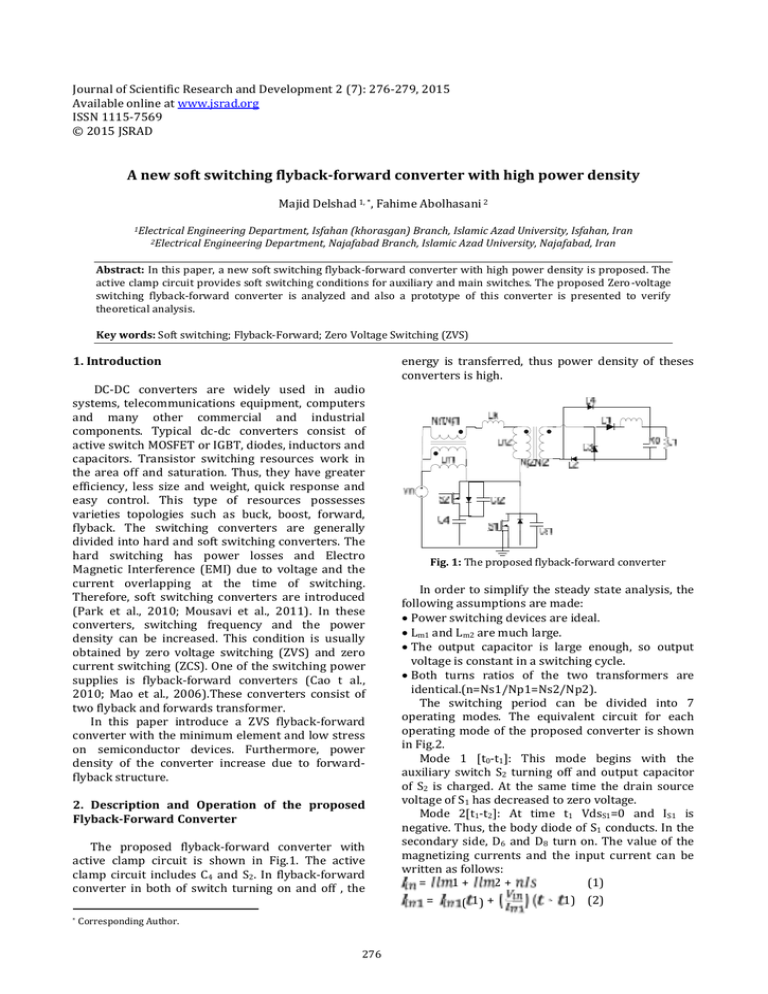
Journal of Scientific Research and Development 2 (7): 276-279, 2015 Available online at www.jsrad.org ISSN 1115-7569 © 2015 JSRAD A new soft switching flyback-forward converter with high power density 1Electrical Majid Delshad 1, *, Fahime Abolhasani 2 Engineering Department, Isfahan (khorasgan) Branch, Islamic Azad University, Isfahan, Iran Engineering Department, Najafabad Branch, Islamic Azad University, Najafabad, Iran 2Electrical Abstract: In this paper, a new soft switching flyback-forward converter with high power density is proposed. The active clamp circuit provides soft switching conditions for auxiliary and main switches. The proposed Zero-voltage switching flyback-forward converter is analyzed and also a prototype of this converter is presented to verify theoretical analysis. Key words: Soft switching; Flyback-Forward; Zero Voltage Switching (ZVS) 1. Introduction *DC-DC converters are widely used in audio systems, telecommunications equipment, computers and many other commercial and industrial components. Typical dc-dc converters consist of active switch MOSFET or IGBT, diodes, inductors and capacitors. Transistor switching resources work in the area off and saturation. Thus, they have greater efficiency, less size and weight, quick response and easy control. This type of resources possesses varieties topologies such as buck, boost, forward, flyback. The switching converters are generally divided into hard and soft switching converters. The hard switching has power losses and Electro Magnetic Interference (EMI) due to voltage and the current overlapping at the time of switching. Therefore, soft switching converters are introduced (Park et al., 2010; Mousavi et al., 2011). In these converters, switching frequency and the power density can be increased. This condition is usually obtained by zero voltage switching (ZVS) and zero current switching (ZCS). One of the switching power supplies is flyback-forward converters (Cao t al., 2010; Mao et al., 2006).These converters consist of two flyback and forwards transformer. In this paper introduce a ZVS flyback-forward converter with the minimum element and low stress on semiconductor devices. Furthermore, power density of the converter increase due to forwardflyback structure. 2. Description and Operation of the proposed Flyback-Forward Converter The proposed flyback-forward converter with active clamp circuit is shown in Fig.1. The active clamp circuit includes C4 and S2. In flyback-forward converter in both of switch turning on and off , the * Corresponding Author. 276 energy is transferred, thus power density of theses converters is high. Fig. 1: The proposed flyback-forward converter In order to simplify the steady state analysis, the following assumptions are made: Power switching devices are ideal. Lm1 and Lm2 are much large. The output capacitor is large enough, so output voltage is constant in a switching cycle. Both turns ratios of the two transformers are identical.(n=Ns1/Np1=Ns2/Np2). The switching period can be divided into 7 operating modes. The equivalent circuit for each operating mode of the proposed converter is shown in Fig.2. Mode 1 [t0-t1]: This mode begins with the auxiliary switch S2 turning off and output capacitor of S2 is charged. At the same time the drain source voltage of S1 has decreased to zero voltage. Mode 2[t1-t2]: At time t1 VdsS1=0 and IS1 is negative. Thus, the body diode of S1 conducts. In the secondary side, D6 and D8 turn on. The value of the magnetizing currents and the input current can be written as follows: = 1+ 2+ (1) = ( − 1) (2) ( 1) + Majid Delshad, Fahime Abolhasani / Journal of Scientific Research and Development, 2 (7) 2015, Pages: 276-279 = ( 1) + ( ) ( − 1) the secondary side, D3 and D4 turn on. The value of the magnetizing currents and the input current are : ( ) = = ( )− ( − ) (3) = (4) = (5) Mode 3 [t2-t3]: The main switch can be turned on under ZVS condition. In this mode the circuit operation is like the circuit operation in mode 2. Mode 4[t3-t4]: This mode begins when D6 turns off and at time t4, S1 is turned off. . The value of the main switch current is: = + (6) Mode 5 [t4-t5]: Input current Iin charges the output capacitor CS1 and discharges CS2.At time t5, the drain-to-source voltage of S2 is zero. Mode 6 [t5-t6]: This mode starts, when Is2 is negative. Thus, the body diode of S2 is conducting. In ( ) + )−( + ) ( − ) = + (7) =− (8) Mode 7 [t6-t7]: The auxiliary switch can be turned on under ZVS condition. In this mode the circuit operation is like the circuit operation in mode 2.When the transformer is demagnetized and the current through L is still not zero, the inductor current still decreases. Mode8 [t7-t8]: This mode begins when the diode D1 turns off. At the end of this mode the auxiliary switch, D3 and D4 turning off. ( D4 Lk D1 Lm2 Lm1 D3 1:m Iin D2 Vin S2 C4 IS2 S1 Fig. 2:The equivalent circuit for each operating mode of the proposed converter 277 Ro C1 Majid Delshad, Fahime Abolhasani / Journal of Scientific Research and Development, 2 (7) 2015, Pages: 276-279 3. The simulation and experimental results In this section a prototype of proposed flybackforward converter at frequency 100 kHz was simulated by PSPICE and Implemented. Elements and specific values of the proposed flyback-forward converter are presented in table I. The key waveforms of proposed converter are shown in Fig. 3. Fig. 4 and Fig 5 show the drain-source voltage and current of main and auxiliary switches respectively. As you can see the both switches, turn on under ZVS conditions because current is negative in turn on instant and therefore body diode of switches conduct. The efficiency of the proposed converter is shown in Fig. 6. Fig. 5: Measured drain-source voltage (red) and current (blue) waveforms of auxiliary switch 100 Table 1: Power stage Components COMPONENTS PARTNAME/VALUE S1,S2 IRF640 L1 100UH D1-D4 MUR860 N,m 1:1 Lk 4.5UH CO 100UF 95 efficiency 90 85 80 75 70 20 30 40 50 60 70 80 90 100 power Fig.6: The efficiency of the proposed converter versus the output power 4. Conclusion In this paper, a flyback-forward converter with active clamp is presented. A ZV condition is provided for turning on and off of the main and auxiliary switches by auxiliary circuit. The coupled inductor in input increase voltage gain and clamp capacitor absorb voltage spike due to leakage inductance of transformer. Also power density of converter is high because the power transfers to the output in on and off state of main switch. Fig.3: The simulated waveforms of drain-source voltage and current of S1 and S2 References A.Mousavi, M.Pahlevaninezhad, P.Das, P.Jain ,”ZCS PWM bidirectional converter with one auxiliary switch”, IEEE, Energy Conversion Congress and Exposition (ECCE), pp.1175-1180, September 2011 Fig. 4: Measured drain-source voltage (blue) and current (yellow) waveforms of main switch E.Adib, H.Farzanehfard,”New zero voltage switching Pwm flyback converter ,” Power Electronic & Drive System & Technologies Conference (PEDSTC), pp.196-200, February 2010. 278 F.Cao, Y.Wang, J.Suo, C.Qi, Q.Tu,”Performance Analysis and Circuit Design of an Interleaved Majid Delshad, Fahime Abolhasani / Journal of Scientific Research and Development, 2 (7) 2015, Pages: 276-279 Active Clamp zero Voltage Switching FlybackForward Boost Converter”, IECON Conference on IEEE Industrial Electronics Society, pp.639-643, November 2010. H.Mao, O.Abdel-Rahman, B.Higgins, G.Potter,”softSwitched Asymmetric half-Bridge flybackForward DC/DC Converter”, Applied Power Electronics Conference and Exposition (APEC), pp.528-532, March 2006. M.Jabbari, H.Farzanehfard,”Analysis and Experimental Results of Switched-ResonatorBased Buck-boost and Inverting-buck Converters”, IEEE International Symposium on Power Electronics for Distributed Generation System (PEDG). Pp.412-416, June 2010. N.Mohan, T.M. Undeland, W.P.Robbins,”Power electronics”, 3rd ed. New York: wiley, 2003. S.H.Park, G.R.Cha, Y.C.Jung, C.Y.Won,”Design and application for PV generation system using a soft switching boost converter with SARC”, IEEE Trans. On Industrial Electronics, Vol.57, No.2, pp.515-522, February 2010. W.Huang, G.Moschopoulos,”A new family of zerovoltage-transition PWM converters with dual active auxiliary circuit”, IEEE Trans. On Power Electron, Vol.21, No.2, pp. 370-379, March 2006. 279
