Relate ADC Topologies And Performance To Applications
advertisement
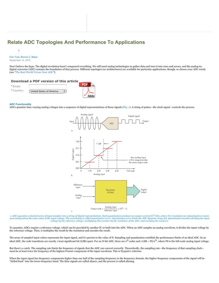
Relate ADC Topologies And Performance To Applications 0 Don Tuite, Bonnie C. Baker September 14, 2012 Don’t believe the hype. The digital revolution hasn’t conquered everything. We still need analog technologies to gather data and turn it into ones and zeroes, and the analog-todigital converter (ADC) remains the foundation of that process. Different topologies (or architectures) are available for particular applications, though, so choose your ADC wisely (see “The Real World Versus Your ADC”). Download a PDF version of this article * Email: * Country: United States of America ADC Functionality ADCs quantize time-varying analog voltages into a sequence of digital representations of those signals (Fig. 1). A string of pulses—the clock signal—controls the process. 1. ADCs quantize a clocked series of input samples into a string of digital representations. Each quantization produces an output word of (2N) bits, where N is resolution (a). Quantization creates uncertainty about the exact value of the input voltage. The uncertainty is called quantization error. Quantization error limits the ADC dynamic range (b). Quantization involves dividing the input voltage by the reference voltage, multiplying that number by the resolution of the ADC, and encoding the result (c). To quantize, ADCs require a reference voltage, which can be provided by another IC or built into the ADC. When an ADC samples an analog waveform, it divides the input voltage by the reference voltage. Then, it multiplies the result by the resolution and encodes the result. The array of sampled input values represents the input signal, and it’s precise to the value of N. Sampling and quantization establish the performance limits of an ideal ADC. In an ideal ADC, the code transitions are exactly 1 least significant bit (LSB) apart. For an N-bit ADC, there are 2N codes and 1 LSB = FS/2N, where FS is the full-scale analog input voltage. But there’s a catch. The sampling rate limits the frequency of signals that the ADC can convert correctly. Theoretically, the sampling rate—the frequency of that sampling clock— must be at least twice the frequency of the highest Fourier component of the input waveform. This is Nyquist’s criterion. When the input signal has frequency components higher than one half of the sampling frequency in the frequency domain, the higher-frequency components of the signal will be “folded back” into the lower-frequency band. The false signals are called aliases, and the process is called aliasing. When aliasing is undesirable, it can be dealt with by applying low-pass filtering to the input signal to remove its higher-frequency components of the input. Building a filter with infinite “brick-wall” rolloff characteristics above the Nyquist frequency is impossible, so anti-aliasing filters should be designed for a cutoff frequency of at least four times Nyquist. Aliasing can be desirable in communications systems precisely because it allows digital extraction (demodulation) of those higher-frequency signals. This technique is known as undersampling. An ADC used for undersampling must have enough input bandwidth and dynamic range to acquire the highest frequency signals of interest. Real ADCs can’t duplicate ideal ADC performance. That’s why ADC data sheets have so many ac and dc performance specifications (see the table and Figure 2). 2. DNL error is the deviation between any two adjacent codes from the ideal (a). INL error is the deviation of an actual code transition from its position on an ideal ADC transfer function (b). SFDR is the ratio of the input signal’s fundamental frequency’s amplitude to that of the largest spurious signal in a given bandwidth (c). Flash ADCs An “N-bit flash” or “parallel-architecture” ADC employs an array of 2N – 1 comparators (Fig. 3). The analog signal is applied simultaneously to each comparator, and each comparator has a different reference voltage on its other input, with the voltages ascending in voltage increments equivalent to 1 LSB. A resistive voltage divider generates the reference voltages, so they’re as precise as the precision of the resistors. 3. Flash ADCs feed the sampled input signal simultaneously to multiple comparators with reference voltages determined by a voltage-divider string. For each quantization event, all the comparators are clocked simultaneously. Comparators with reference voltages below the analog generate a digital one. Comparators with reference voltages equal to or above the analog generate a digital zero. The result is a “thermometer code” representation of the input signal. Output logic in the ADC converts this representation to standard binary code. Flash ADCs are very fast because they generate an output in one ADC for every clock cycle. They are generally more expensive because of their circuit complexity. Pipelined (Subranging) ADCs As a tradeoff to that complexity, pipelined ADCs reduce the number of comparators while adding clock cycles to the conversion process (Fig. 4). They quantize in two or more stages. Each stage comprises a sample-and-hold (S/H) circuit, a flash ADC with “M” bits of resolution, and a digital-to-analog converter (DAC). The output of an S/H circuit is a voltage that “locks in” the voltage on its input at the time it receives a trigger signal. 4. Pipelined ADCs use multiple stages, each comprising a sample-and-hold, a flash ADC with a few bits of resolution, and a DAC, which is fed by the output of the stage before it. Each time, the output of the DAC is subtracted from the input of the prior stage. In the first stage of a pipelined ADC, the S/H samples the analog signal, and the flash ADC converts it to an M-bit digital code. This code represents the most significant bits (MSBs) of the ADC’s final output. The same code is fed to the DAC, which converts code to an analog voltage. This voltage is subtracted from the voltage held by the S/H. The next stage in the pipeline samples and converts the resulting voltage. The number of stages depends on the required resolution and the resolution of the flash ADCs used in each stage. In theory, the resolution of the ADC should be the sum of the resolutions of the flash ADCs. In practice, some bits are used for error correction. Pipeline ADCs are not as fast as flash ADCs, but they achieve higher resolutions and dynamic range. In communications systems, wide input bandwidths permit undersampling. The need to make a sequence of conversions causes a delay (latency) between the time a signal is sampled and the time its digital representation appears on the output. Sigma-Delta ADCs Sigma-delta ADCs feature a sigma-delta modulator and a 1-bit DAC. The sigma-delta modulator consists of an analog integrator and a comparator, with feedback through a 1-bit DAC (Fig. 5). The DAC’s output is subtracted from the analog input signal voltage. The resulting difference voltage is fed to the integrator and the comparator. The other input to the comparator is a reference voltage. The output of the comparator is a 1-bit digital output, which drives the DAC. 5. SAR converters compare the analog input voltage against a descending series of voltages (1, 1/2, 1/4, 1/8, 1/16... 1/2N times the reference, up to the resolution of the ADC) and accumulate the results. The process is clocked at a very fast “oversampled rate,” although the actual quantization time is comparatively long because the binary output stream from the comparator is a serial succession of ones and zeros. The ratio of ones to zeros is a function of the input signal’s amplitude. A binary output representing the value of the analog input is obtained by digitally filtering and decimating this stream of one and zeroes. That’s the part that takes all the time. But speed isn’t the important feature of sigma-deltas. Resolution is. Sigma-delta ADCs can have resolutions as high as 24 bits. Also, oversampling reduces requirements for anti-alias filtering. Conversely, thanks to oversampling, sigma-delta ADCs also allow a technique called noise shaping, in which high-frequency noise components on the input signal are shifted up in frequency and digitally filtered from the output of the ADC. DT and CT Sigma Deltas There are two sigma-delta architectures: discrete time (DT) and continuous time (CT). Typical resolutions for DT converters range from 16 to 24 bits with input bandwidths of up to 5 MHz. CT converters deliver 12 to 16 bits with input bandwidths of up to 25 MHz. They also have built-in anti-aliasing. Architecturally, CT sigma-deltas add a continuous-time noise-shaping filter (NSF) ahead of the integrator (Fig. 5, again). Successive Approximation ADCs Successive approximation (SAR) converters compare the analog input voltage against a series of successively smaller voltages (Fig. 6). Each voltage represents one of the bits in the digital output code. These voltages are fractions of the full-scale input voltage (1/2, 1/4, 1/8, 1/16... 1/2N, where N = number of bits). 6. For each sampling period, a sigma-delta ADC outputs a serial bit stream that’s converted to a representation of the input signal by digitally filtering and decimating the stream. The first comparison is made between the analog input voltage and a voltage representing the MSB. If that analog input voltage is greater than the MSB voltage, the value of the MSB is set to 1. If it isn’t greater than the MSB voltage, it’s set to 0. The second comparison is made between the analog input voltage and a voltage representing the sum of the MSB and the next MSB. The value of the second MSB is then set accordingly. The third comparison is made between the analog input voltage and the voltage representing the sum of the three MSBs. The process repeats until the value of the LSB is established. SAR converters can be built on a small area of silicon. This makes them inexpensive to manufacture. To achieve N bits of resolution, they require N comparison steps. This requires more time than a pipelined ADC. Tags: ADC analog-to-digital converter applications Architecture Basics Engineering Essentials topology tutorial Like 0 Tweet * Email Address: Share * Country: Please select one * Select your eNewsletter options below: .. ED Update - Industry-wide News (weekly) Embedded Update - Industry Specific News (weekly)
