DATASHEET
High Performance 1A LDO
ISL78310
Features
The ISL78310 is a low dropout voltage, high-current, single
output LDO specified for 1A output current. This part operates
from input voltages down to 2.2V and up to 6V. The part offers
fixed and external resistor adjustable output voltages from 0.8V
to 5V. Custom voltage options are available upon request.
• 2.2V to 6V input supply
For applications that desire to set the in-rush current to less than
the current limit of the part, or for applications that require
turn-on time control, an external capacitor can be placed on the
soft-start pin for maximum control. A supply-independent
ENABLE signal allows the part to be placed into a low quiescent
current shutdown mode. Sub-micron CMOS process is used for
this product family to deliver best-in-class analog performance
and overall value.
• Adjustable in-rush current limiting
• 130mV dropout voltage typical (at 1A)
• Fast load transient response
• ±0.2% initial VOUT accuracy
• 58dB typical PSRR
• 63µVRMS output noise at VOUT = 1.8V
• Power-good feature
• 500mV feedback voltage
• Supply-independent 1V enable input threshold
• Short-circuit current protection
This CMOS LDO consumes significant lower quiescent (ground pin)
current as a function of load over bipolar LDOs, which translates into
higher efficiency and packages with smaller footprints. Quiescent
current is optimized to achieve a very fast load transient response.
• 1A peak reverse current
• Over-temperature shutdown
• Any cap stable with minimum 10µF ceramic
The ISL78310 is AEC-Q100 rated. The ISL78310 is rated for the
automotive temperature range (-40°C to +125°C).
• ±1.8% guaranteed VOUT accuracy for junction temperature
range from -40°C to +125°C
Applications
• Available in a 10 Lead DFN package
• Core & I/O power
• Pb-free (RoHS compliant)
• Camera modules
• AEC-Q100 qualified
• Post regulation of switched supplies
• Radio systems
• Infotainment systems
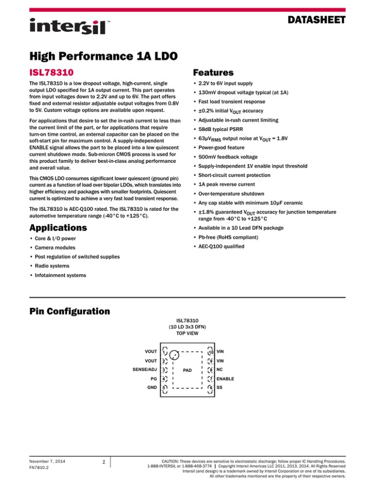
Pin Configuration
ISL78310
(10 LD 3x3 DFN)
TOP VIEW
November 7, 2014
FN7810.2
1
VOUT
1
10 VIN
VOUT
2
9 VIN
SENSE/ADJ
3
PG
4
7 ENABLE
GND
5
6 SS
PAD
8 NC
CAUTION: These devices are sensitive to electrostatic discharge; follow proper IC Handling Procedures.
1-888-INTERSIL or 1-888-468-3774 | Copyright Intersil Americas LLC 2011, 2013, 2014. All Rights Reserved
Intersil (and design) is a trademark owned by Intersil Corporation or one of its subsidiaries.
All other trademarks mentioned are the property of their respective owners.
ISL78310
Pin Descriptions
PIN #
PIN NAME
DESCRIPTION
1, 2
VOUT
3
SENSE/ADJ
For internally fixed VOUT option, this pin provides output voltage feedback. By connecting this pin to the output rail
at the load, small voltage drops caused by PCB trace resistance can be eliminated.
For the adjustable output voltage option, this pin is connected to the feedback resistor divider and provides voltage
feedback signals for the LDO to set the output voltage.
4
PG
This is an open drain logic output used to indicate the status of the output voltage. Logic low indicates VOUT is not
in regulation. Must be grounded if not used.
5
GND
6
SS
7
ENABLE
8
NC
Do not connect this pin to ground or supply. Leave floating.
9, 10
VIN
Input supply pin. A minimum 10µF X5R/X7R input capacitor is required for stability. See “External Capacitor
Requirements” on page 9 for more details.
Regulated output voltage. A minimum 10µF X5R/X7R output capacitor is required for stability. See “External
Capacitor Requirements” on page 9 for more details.
Ground.
External capacitor on this pin adjusts start-up ramp and controls in-rush current.
VIN independent chip enable. TTL and CMOS compatible.
EPAD
EPAD at ground potential. Soldering it directly to GND plane is required for thermal considerations. See “Heatsinking
the DFN Package” on page 12 for more details.
Ordering Information
PART NUMBER
(Notes 1, 3, 4)
ISL78310ARAJZ
PART
MARKING
VOUT VOLTAGE
(Note 2)
TEMP
RANGE (°C)
ADJ
-40 to +125
DZAE
PACKAGE
(Pb-Free)
10 Ld 3x3 DFN
PKG
DWG. #
L10.3x3
NOTES:
1. Add “-T*” suffix for tape and reel. Please refer to TB347 for details on reel specifications.
2. For other output voltages, contact Intersil Marketing.
3. These Intersil Pb-free plastic packaged products employ special Pb-free material sets, molding compounds/die attach materials, and 100% matte
tin plate plus anneal (e3 termination finish, which is RoHS compliant and compatible with both SnPb and Pb-free soldering operations). Intersil
Pb-free products are MSL classified at Pb-free peak reflow temperatures that meet or exceed the Pb-free requirements of IPC/JEDEC J STD-020.
4. For Moisture Sensitivity Level (MSL), please see device information page for ISL78310. For more information on MSL please see techbrief TB363.
Submit Document Feedback
2
FN7810.2
November 7, 2014
ISL78310
Typical Application Diagrams
9
2.5V ± 10%
10
10µF
VIN
VIN
V OUT
1
V OUT
2
SENSE/ADJ
1.8V ± 1.8%
10µF
3
100k
10k
ISL78310
7
6
ENABLE
PG
4
SS
(Note 5)
GND
5
FIGURE 1. FIXED TYPICAL APPLICATION DIAGRAM
9
2.5V ± 10%
10µF
10
VIN
VIN
V OUT
ISL78310
V OUT
1
2
1.8V ± 1.8%
10µF
2.6k
10k
100k
SENSE/ADJ
1k
7
6
ENABLE
PG
4
SS
GND
(Note 5)
5
FIGURE 2. ADJUSTABLE TYPICAL APPLICATION DIAGRAM
NOTE:
5. Used when large bulk capacitance required on VOUT for application.
Submit Document Feedback
3
FN7810.2
November 7, 2014
ISL78310
ISL78310 Schematic Block Diagram
VIN
VOUT
Submit Document Feedback
4
FN7810.2
November 7, 2014
ISL78310
Absolute Maximum Ratings
Thermal Information
VIN relative to GND (Note 6) . . . . . . . . . . . . . . . . . . . . . . . . . . -0.3V to + 6.5V
VOUT relative to GND (Note 6). . . . . . . . . . . . . . . . . . . . . . . . . -0.3V to + 6.5V
PG, ENABLE, SENSE/ADJ, SS
Relative to GND (Note 6) . . . . . . . . . . . . . . . . . . . . . . . . . . . -0.3V to + 6.5V
Thermal Resistance . . . . . . . . . . . . . . . . . . . . JA (°C/W) JC (°C/W)
10 Ld DFN Package (Notes 7, 8) . . . . . . . .
48
7
Storage Temperature Range. . . . . . . . . . . . . . . . . . . . . . . .-65°C to +150°C
Junction Temperature . . . . . . . . . . . . . . . . . . . . . . . . . . . . . . . . . . . . .+150°C
Pb-Free Reflow Profile . . . . . . . . . . . . . . . . . . . . . . . . . . . . . . . . . . see TB493
Recommended Operating Conditions (Notes 9, 10)
Junction Temperature Range (TJ) (Note 9) . . . . . . . . . . . .-40°C to +125°C
VIN relative to GND. . . . . . . . . . . . . . . . . . . . . . . . . . . . . . . . . . . . . .2.2V to 6V
VOUT range . . . . . . . . . . . . . . . . . . . . . . . . . . . . . . . . . . . . . . . . . 800mV to 5V
PG, ENABLE, SENSE/ADJ, SS relative to GND . . . . . . . . . . . . . . .0V to + 6V
PG Sink Current . . . . . . . . . . . . . . . . . . . . . . . . . . . . . . . . . . . . . . . . . . <10mA
ESD Rating
Human Body Model (Tested per JESD22-A114E) . . . . . . . . . . . . . . . . .2.5kV
Machine Model (Tested per JESD-A115-A) . . . . . . . . . . . . . . . . . . . . . 250V
Charge Device Model (Tested per AEC-Q100-011) . . . . . . . . . . . . . . . . . 1kV
CAUTION: Do not operate at or near the maximum ratings listed for extended periods of time. Exposure to such conditions may adversely impact product
reliability and result in failures not covered by warranty.
NOTES:
6. Absolute maximum voltage rating is defined as the voltage applied for a lifetime average duty cycle above 6V of 1%.
7. JA is measured in free air with the component mounted on a high effective thermal conductivity test board with “direct attach” features. See Tech
Brief TB379.
8. For JC, the “case temp” location is the center of the exposed metal pad on the package underside.
9. Extended operation at these conditions may compromise reliability. Exceeding these limits will result in damage. Recommended operating conditions
define limits where specifications are guaranteed.
10. Electromigration specification defined as lifetime average junction temperature of +110°C where max rated DC current = lifetime average current.
Electrical Specifications Unless otherwise noted, VIN = VOUT + 0.4V, VOUT = 1.8V, CIN = COUT = 10µF, TJ = +25°C, ILOAD = 0A.
Applications must follow thermal guidelines of the package to determine worst case junction temperature. Please refer to “ISL78310 Schematic Block
Diagram” on page 4 and Tech Brief TB379. Boldface limits apply across the operating temperature range, -40°C to +125°C.
PARAMETER
SYMBOL
TEST CONDITIONS
MIN
(Note 11)
TYP
MAX
(Note 11)
UNITS
-1.8
0.2
1.8
%
-1.8
0.2
1.8
%
491
500
509
mV
1
%
DC CHARACTERISTICS
DC Output Voltage Accuracy
VOUT
VOUT Options: 0.8V, 1.2V, 1.5V and 1.8V
2.2V VIN < 3.6V; 0A < ILOAD 1A
VOUT Options: 2.5V, 3.3V and 5.0V
VOUT + 0.4V VIN 6V; 0A < ILOAD < 1A
Feedback Pin (ADJ Option Only)
VADJ
2.2V VIN 6V, 0A < ILOAD < 1A
DC Input Line Regulation
VOUT/
VIN
VOUT + 0.5V < VIN < 5V
DC Output Load Regulation
VOUT/
IOUT
0A < ILOAD < 1A, All voltage options
Feedback Input Current
VADJ = 0.5V
Ground Pin Current
IQ
-1
%
0.01
1
µA
ILOAD = 0A, 2.2V < VIN < 6V
3
5
mA
ILOAD = 1A, 2.2V < VIN < 6V
5
7
mA
ENABLE Pin = 0V, VIN = 6V
0.2
12
µA
Dropout Voltage (Note 12)
VDO
ILOAD = 1A, VOUT = 2.5V
130
212
mV
Output Short Circuit Current
OCP
VOUT = 0V, 2.2V < VIN < 6V
1.75
A
Thermal Shutdown Temperature
TSD
2.2V < VIN < 6V
160
°C
Thermal Shutdown Hysteresis
(Rising Threshold)
TSDn
2.2V < VIN < 6V
30
°C
PSRR
f = 1kHz, ILOAD = 1A; VIN = 2.2V
58
dB
f = 120Hz, ILOAD = 1A; VIN = 2.2V
72
dB
ILOAD = 1A, BW = 10Hz < f < 100kHz
63
µVRMS
Ground Pin Current in Shutdown
ISHDN
AC CHARACTERISTICS
Input Supply Ripple Rejection
Output Noise Voltage
Submit Document Feedback
5
FN7810.2
November 7, 2014
ISL78310
Electrical Specifications Unless otherwise noted, VIN = VOUT + 0.4V, VOUT = 1.8V, CIN = COUT = 10µF, TJ = +25°C, ILOAD = 0A.
Applications must follow thermal guidelines of the package to determine worst case junction temperature. Please refer to “ISL78310 Schematic Block
Diagram” on page 4 and Tech Brief TB379. Boldface limits apply across the operating temperature range, -40°C to +125°C. (Continued)
PARAMETER
SYMBOL
TEST CONDITIONS
MIN
(Note 11)
TYP
MAX
(Note 11)
UNITS
ENABLE PIN CHARACTERISTICS
Turn-on Threshold
2.2V < VIN < 6V
0.3
0.8
1
V
Hysteresis (Rising Threshold)
2.2V < VOUT + 0.4V < 6V
10
80
200
mV
1
µA
Enable Pin Turn-on Delay
COUT = 10µF, ILOAD = 1A
Enable Pin Leakage Current
VIN = 6V, EN = 3V
100
µs
ADJUSTABLE INRUSH CURRENT LIMIT CHARACTERISTICS
Current limit adjust
IPD
VIN = 3.5V, EN = 0V, SS = 1V
ICHG
0.5
1
1.3
mA
-3.3
-2
-0.8
µA
75
85
92
%VOUT
PG PIN CHARACTERISTICS
VOUT PG Flag Threshold
VOUT PG Flag Hysteresis
4
PG Flag Low Voltage
VIN = 2.5V, ISINK = 500µA
PG Flag Leakage Current
VIN = 6V, PG = 6V
%
100
mV
1
µA
NOTES:
11. Compliance to datasheet limits is assured by one or more methods: production test, characterization and/or design.
12. Dropout is defined by the difference in supply VIN and VOUT when the supply produces a 2% drop in VOUT from its nominal value.
Submit Document Feedback
6
FN7810.2
November 7, 2014
ISL78310
Typical Operating Performance
IL = 0A.
Unless otherwise noted: VIN = 2.2V, VOUT = 1.8V, CIN = COUT = 10µF, TJ = +25°C,
2.0
1.8
1.8
1.2
1.6
1.4
VOUT (V)
VOUT (%)
0.6
0
-0.6
1.2
+125°C
1.0
0.8
-40°C
+25°C
0.6
0.4
-1.2
0.2
-1.8
-50
-25
0
25
50
75
100
125
0
150
0
1
3
2
4
SUPPLY VOLTAGE (V)
JUNCTION TEMPERATURE (°C)
1.8
5
+25°C
0.6
VOUT (%)
GROUND CURRENT (mA)
1.2
0
-0.6
-40°C
+125°C
-1.2
-1.8
0
0.25
0.50
0.75
4
3
2
1
0
1.00
3
2
FIGURE 5. VOUT vs LOAD CURRENT
200
180
DROPOUT VOLTAGE (mV)
+125°C
3.00
2.75
+25°C
6
FIGURE 6. GROUND CURRENT vs SUPPLY VOLTAGE
3.50
3.25
5
4
INPUT VOLTAGE (V)
LOAD CURRENT (A)
GROUND CURRENT (mA)
6
FIGURE 4. VOUT vs SUPPLY VOLTAGE
FIGURE 3. VOUT vs TEMPERATURE
-40°C
2.50
2.25
2.00
1.75
1.50
5
VOUT = 2.5V
ILOAD = 1A
160
140
120
ILOAD = 500mA
100
80
ILOAD = 100mA
60
40
20
0
0.25
0.50
0.75
LOAD CURRENT (A)
FIGURE 7. GROUND CURRENT vs LOAD CURRENT
Submit Document Feedback
7
1.00
0
-40 -25 -10
5
20
35
50
65
80
95 110 125
TEMPERATURE (°C)
FIGURE 8. DROPOUT VOLTAGE vs TEMPERATURE
FN7810.2
November 7, 2014
ISL78310
Typical Operating Performance
IL = 0A. (Continued)
Unless otherwise noted: VIN = 2.2V, VOUT = 1.8V, CIN = COUT = 10µF, TJ = +25°C,
VOLTAGE RAILS AT 50mV/DIV
VIN = 3.7V, VOUT = 3.3V, COUT = 10µF, CPB = 100pF
VIN = 2.9V, VOUT = 2.5V, COUT = 10µF, CPB = 82pF
VIN = 2.5V, VOUT = 1.8V, COUT = 10µF, CPB = 82pF
VIN = 2.5V, VOUT = 1.5V, COUT = 22µF, CPB = 150pF
VIN = 2.5V, VOUT = 1.2V, COUT = 47µF, CPB = 270pF
VIN = 2.5V, VOUT = 1.0V, COUT = 47µF, CPB = 220pF
1A
1mA
di/dt = 4A/µs
20µs/DIV
FIGURE 9. LOAD TRANSIENT RESPONSE
90
80
ENABLE
(2V/DIV)
500mA
1A
70
60
PSRR (dB)
VOUT (1V/DIV)
50
100mA
0mA
40
30
SS (1V/DIV)
20
(500µs/DIV)
10
PG (1V/DIV)
FIGURE 10. ENABLE START-UP
Submit Document Feedback
8
0
100
VIN = 2.5V, VOUT = 1.8V, COUT = 10µF, CPB = 82pF
1k
10k
FREQUENCY (Hz)
100k
1M
FIGURE 11. PSRR vs FREQUENCY
FN7810.2
November 7, 2014
ISL78310
Typical Operating Performance
IL = 0A. (Continued)
Unless otherwise noted: VIN = 2.2V, VOUT = 1.8V, CIN = COUT = 10µF, TJ = +25°C,
SPECTRAL NOISE DENSITY (µV/√Hz)
10
1
0.1
0.01
ILOAD = 1A
0.001
10
100
1k
10k
100k
1M
10M
FREQUENCY (Hz)
FIGURE 12. SPECTRAL NOISE DENSITY vs FREQUENCY
Applications Information
Phase Boost Capacitor (CPB)
Input Voltage Requirements
A small phase boost capacitor, CPB, can be placed across the top
resistor in the feedback resistor divider network (Figure 13) in
order to place a zero at:
The ISL78310 is capable of delivering output voltages from 0.8V
to 5.0V. Due to the nature of an LDO, VIN must be some margin
higher than the output voltage plus dropout at the maximum
rated current of the application if active filtering (PSRR) is
expected from VIN to VOUT. The generous dropout specification of
this family of LDOs allows applications to design for a level of
efficiency that can accommodate profiles smaller than the
TO220/263.
External Capacitor Requirements
This zero increases the crossover frequency of the LDO and
provides additional phase resulting in faster load transient
response.
VIN
VOUT
PG
EN
GENERAL GUIDELINE
External capacitors are required for proper operation. Careful
attention must be paid to layout guidelines and selection of
capacitor type and value to ensure optimal performance.
(EQ. 1)
F Z = 1 2 pi R TOP C PB
CPB
ISL78310
RTOP
ADJ
CIN
COUT
RBOTTOM
SS
OUTPUT CAPACITOR
The ISL78310 applies state of the art internal compensation to
keep the selection of the output capacitor simple for the
customer. Stable operation over full temperation, VIN range, VOUT
range and load extremes are guaranteed for all capacitor types
and values assuming a minimum of 10µF X5R/X7R is used for
local bypass on VOUT. This output capacitor must be connected to
the VOUT and GND pins of the LDO with PCB traces no longer than
0.5cm. Additional capacitors of any value in ceramic, POSCAP,
alum/tantalum electrolytic types may be placed in parallel to
improve PSRR at higher frequencies and/or load transient AC
output voltage tolerances.
FIGURE 13.
It is also important to note that the LDO stability and load transient
are affected by the type of output capacitor used. For optimal
result, empirical tuning of CPB is suggested for each specific
application. It is recommended to not use CPB when high ESR
capacitors such as aluminum electrolytic or tantalum are used.
Table 1 shows the recommended CPB, RTOP, RBOTTOM and CPB
values for different output voltage rails.
INPUT CAPACITOR
For proper operation, a minimum capacitance of 10µF X5R/X7R
is required at the input. This ceramic input capacitor must be
connected to VIN and GND pins of the LDO with PCB traces no
longer than 0.5cm.
Submit Document Feedback
9
FN7810.2
November 7, 2014
ISL78310
Functional Description
TABLE 1.
VOUT
(V)
RTOP
(kΩ)
RBOTTOM
(Ω)
CPB
(pF)
COUT
(µF)
5.0
2.61
287
100
10
3.3
2.61
464
100
10
2.5
2.61
649
82
10
1.8
2.61
1.0k
82
10
1.5*
2.61
1.3k
68
10
Enable Operation
The Enable turn-on threshold is typically 0.8V with a hysteresis of
80mV. The Enable pin does not have an internal pull-up or
pull-down resistor. As a result, this pin must not be left floating.
This pin must be tied to VIN if it is not used. A pull-up resistor
(typically 1k to 10kwill be required for applications that use
open collector or open drain outputs to control the Enable pin.
The Enable pin may be connected directly to VIN for applications
that are always on.
1.5
2.61
1.3k
150
22
1.2*
2.61
1.87k
120
22
1.2*
2.61
1.87k
270
47
Soft-Start Operation
1.0
2.61
2.61k
220
47
0.8
2.61
4.32k
220
47
The soft-start circuit controls the rate at which the output voltage
rises up to regulation at power-up or LDO enable. This start-up
ramp time can be set by adding an external capacitor from the
SS pin to GND. An internal 2µA current source charges up this
CSS and the feedback reference voltage is clamped to the
voltage across it. The start-up time of the regulator output
voltage for a given CSS value can be calculated using Equation 2.
*Either option could be used, depending on cost/performance
requirements.
Thermal Fault Protection
In the event the die temperature exceeds typically +160°C, then
the output of the LDO shuts down until the die temperature cools
down to typically +130°C. The level of power, combined with the
thermal resistance of the package (+48°C/W for DFN),
determines whether the junction temperature exceeds the
thermal shutdown temperature specified in the “Electrical
Specifications” on page 5 (see thermal packaging guidelines).
Current Limit Protection
The ISL78310 LDO incorporates protection against overcurrent
due to any short or overload condition applied to the output pin.
The current limit circuit performs as a constant current source
when the output current exceeds the current limit threshold
noted in the “Electrical Specifications” on page 5. If the short or
C SS x0.5V
t RAMP = ---------------------------2A
(EQ. 2)
The soft-start function also effectively limits the amount of
in-rush current to less than the programmed current limit during
start-up or an enable sequence, to avoid an overcurrent fault
condition. This can be an issue for applications that require large,
external bulk capacitances on VOUT where high levels of charging
current can be seen for a significant period of time. High in-rush
currents can cause VIN to drop below minimum, which could
cause VOUT to shutdown.
overload condition is removed from VOUT, then the output returns
to normal voltage mode regulation. In the event of an overload
condition on the DFN package, the LDO will begin to cycle on and
off due to the die temperature exceeding thermal fault condition.
Submit Document Feedback
10
FN7810.2
November 7, 2014
ISL78310
IOUT (1A/DIV)
IOUT (1A/DIV)
VOUT (1V/DIV)
VOUT (1V/DIV)
TIME (1ms/DIV)
TIME (2ms/DIV)
FIGURE 14. IN-RUSH CURRENT WITH NO CSS, COUT = 1000µF,
IN-RUSH CURRENT = 1.8A
FIGURE 15. IN-RUSH CURRENT WITH CSS = 15nF, COUT = 1000µF,
IN-RUSH CURRENT = 0.5A
IOUT (1A/DIV)
VOUT (1V/DIV)
TIME (2ms/DIV)
FIGURE 16. IN-RUSH CURRENT WITH CSS = 33nF, COUT = 1000µF, IN-RUSH CURRENT = 0.2A
Equation 3 can be used to calculate CSS for a desired in-rush
current, where VOUT is the output voltage, COUT is the total
capacitance on the output, and IINRUSH is the desired in-rush
current.
V OUT xC OUT x2A
C SS = --------------------------------------------------------I INRUSH x0.5V
(EQ. 3)
The scopes in Figures 14, 15 and 16 capture the response for the
soft-start function. The output voltage is set to 1.8V.
The external capacitor is always discharged to ground at the
beginning of start-up or enabling.
Power-Good Operation
The PGOOD is a logic output that indicates the status of VOUT.
The PGOOD flag is an open-drain NMOS that can sink 10mA
during a fault condition. The PGOOD pin requires an external
pull-up resistor, which is typically connected to the VOUT pin. The
PGOOD pin should not be pulled up to a voltage source greater
than VIN. The PGOOD goes low when the output voltage drops
below 84% of the nominal output voltage or if the part is
Submit Document Feedback
11
disabled. The PGOOD comparator functions during current limit
and thermal shutdown. For applications not using this feature,
connect this pin to ground.
Output Voltage Selection
An external resistor divider is used to scale the output voltage
relative to the internal reference voltage. This voltage is then fed
back to the error amplifier. The output voltage can be
programmed to any level between 0.8V and 5V. An external
resistor divider, R1 and R2, is used to set the output voltage as
shown in Equation 4. The recommended value for R2 is 500 to
1kR1is then chosen according to Equation 5.
R1
V OUT = 0.5V ------- + 1
R2
(EQ. 4)
V OUT
R 1 = R 2 ---------------- – 1
0.5V
(EQ. 5)
FN7810.2
November 7, 2014
ISL78310
Power Dissipation
The junction temperature must not exceed the range specified in
the “Recommended Operating Conditions” on page 5. The power
dissipation can be calculated by using Equation 6:
(EQ. 6)
P D = V IN – V OUT I OUT + V IN I GND
The maximum allowed junction temperature, TJ(MAX), and the
maximum expected ambient temperature, TA(MAX), will
determine the maximum allowable power dissipation, as shown
in Equation 7:
(EQ. 7)
P D MAX = T J MAX – T A JA
JA is the junction-to-ambient thermal resistance.
General Power PAD Design
Considerations
Figure 18 shows the recommended use of vias on the thermal
pad to remove heat from the IC. This typical array populates the
thermal pad footprint with vias spaced three times the radius
distance from the center of each via. Small via size is advisable,
but not to the extent that solder reflow becomes difficult.
All vias should be connected to the pad potential, with low
thermal resistance for efficient heat transfer. Complete
connection of the plated-through hole to each plane is important.
It is not recommended to use “thermal relief” patterns to connect
the vias.
For safe operation, ensure that the power dissipation PD,
calculated from Equation 6, is less than the maximum allowable
power dissipation PD(MAX).
Heatsinking the DFN Package
The DFN package uses the copper area on the PCB as a heat-sink.
The EPAD of this package must be soldered to the copper plane
(GND plane) for heat sinking. Figure 17 shows a curve for the JA
of the DFN package for different copper area sizes.
46
JA (°C/W)
44
42
FIGURE 18. PCB VIA PATTERN
40
38
36
34
2
4
6
8
10
12
14
16
18
20
22
24
EPAD-MOUNT COPPER LAND AREA ON PCB, mm2
FIGURE 17. 3mmx3mm 10 LD DFN ON 4-LAYER PCB WITH THERMAL
VIAS JA vs EPAD-MOUNT COPPER LAND AREA ON PCB
Submit Document Feedback
12
FN7810.2
November 7, 2014
ISL78310
Revision History
The revision history provided is for informational purposes only and is believed to be accurate, but not warranted. Please go to web to make sure you
have the latest Rev.
DATE
REVISION
CHANGE
November 7, 2014
FN7810.2
“Absolute Maximum Ratings” on page 5: Updated CDM testing from: Charged Device Model (Tested per
JESD22-C101E) to Charged Device Model (Tested per AEC Q100-011).
On page 2: Removed part number ISL78310ARAJZ-TR5303 from ordering information table.
Updated POD from rev 6 to rev 9.
December 23, 2013
FN7810.1
Page 12 - 2nd line of the disclaimer changed from:
"Intersil products are manufactured, assembled and tested utilizing ISO9001 quality systems as noted"
to:
"Intersil Automotive Qualified products are manufactured, assembled and tested utilizing TS16949 quality
systems as noted".
February 17, 2011
FN7810.0
Initial Release.
About Intersil
Intersil Corporation is a leading provider of innovative power management and precision analog solutions. The company's products
address some of the largest markets within the industrial and infrastructure, mobile computing and high-end consumer markets.
For the most updated datasheet, application notes, related documentation and related parts, please see the respective product
information page found at www.intersil.com.
You may report errors or suggestions for improving this datasheet by visiting www.intersil.com/ask.
Reliability reports are also available from our website at www.intersil.com/support
For additional products, see www.intersil.com/en/products.html
Intersil Automotive Qualified products are manufactured, assembled and tested utilizing TS16949 quality systems as noted
in the quality certifications found at www.intersil.com/en/support/qualandreliability.html
Intersil products are sold by description only. Intersil Corporation reserves the right to make changes in circuit design, software and/or specifications at any time
without notice. Accordingly, the reader is cautioned to verify that data sheets are current before placing orders. Information furnished by Intersil is believed to be
accurate and reliable. However, no responsibility is assumed by Intersil or its subsidiaries for its use; nor for any infringements of patents or other rights of third
parties which may result from its use. No license is granted by implication or otherwise under any patent or patent rights of Intersil or its subsidiaries.
For information regarding Intersil Corporation and its products, see www.intersil.com
Submit Document Feedback
13
FN7810.2
November 7, 2014
ISL78310
Package Outline Drawing
L10.3x3
10 LEAD DUAL FLAT PACKAGE (DFN)
Rev 9, 10/13
3.00
5
PIN #1 INDEX AREA
A
B
1
5
PIN 1
INDEX AREA
(4X)
3.00
2.00
8x 0.50
2
10 x 0.23
0.10
1.60
TOP VIEW
10x 0.35
BOTTOM VIEW
(4X)
0.10 M C A B
0.415
0.200
0.23
0.35
(10 x 0.55)
SEE DETAIL "X"
(10x 0.23)
1.00
MAX
0.10 C
0.20
2.00
(8x 0.50)
BASE PLANE
C
SEATING PLANE
0.08 C
SIDE VIEW
0.415
C
0.20 REF
4
1.60
0.05
2.85 TYP
TYPICAL RECOMMENDED LAND PATTERN
DETAIL "X"
NOTES:
1.
Dimensions are in millimeters.
Dimensions in ( ) for Reference Only.
2.
Dimensioning and tolerancing conform to ASME Y14.5m-1994.
3.
Unless otherwise specified, tolerance : Decimal ± 0.05
4.
Tiebar shown (if present) is a non-functional feature.
5.
The configuration of the pin #1 identifier is optional, but must be
located within the zone indicated. The pin #1 identifier may be
either a mold or mark feature.
Submit Document Feedback
14
FN7810.2
November 7, 2014
