- The Ohio State University
advertisement
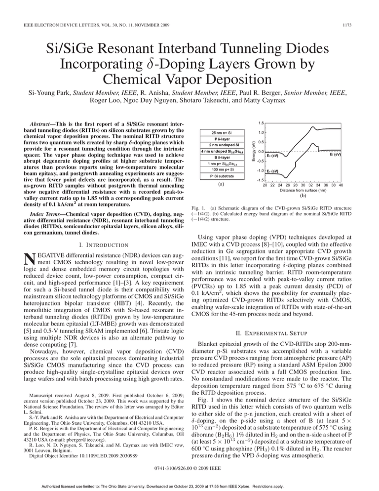
IEEE ELECTRON DEVICE LETTERS, VOL. 30, NO. 11, NOVEMBER 2009 1173 Si/SiGe Resonant Interband Tunneling Diodes Incorporating δ -Doping Layers Grown by Chemical Vapor Deposition Si-Young Park, Student Member, IEEE, R. Anisha, Student Member, IEEE, Paul R. Berger, Senior Member, IEEE, Roger Loo, Ngoc Duy Nguyen, Shotaro Takeuchi, and Matty Caymax Abstract—This is the first report of a Si/SiGe resonant interband tunneling diodes (RITDs) on silicon substrates grown by the chemical vapor deposition process. The nominal RITD structure forms two quantum wells created by sharp δ-doping planes which provide for a resonant tunneling condition through the intrinsic spacer. The vapor phase doping technique was used to achieve abrupt degenerate doping profiles at higher substrate temperatures than previous reports using low-temperature molecular beam epitaxy, and postgrowth annealing experiments are suggestive that fewer point defects are incorporated, as a result. The as-grown RITD samples without postgrowth thermal annealing show negative differential resistance with a recorded peak-tovalley current ratio up to 1.85 with a corresponding peak current density of 0.1 kA/cm2 at room temperature. Index Terms—Chemical vapor deposition (CVD), doping, negative differential resistance (NDR), resonant interband tunneling diodes (RITDs), semiconductor epitaxial layers, silicon alloys, silicon germanium, tunnel diodes. I. I NTRODUCTION N EGATIVE differential resistance (NDR) devices can augment CMOS technology resulting in novel low-power logic and dense embedded memory circuit topologies with reduced device count, low-power consumption, compact circuit, and high-speed performance [1]–[3]. A key requirement for such a Si-based tunnel diode is their compatibility with mainstream silicon technology platforms of CMOS and Si/SiGe heterojunction bipolar transistor (HBT) [4]. Recently, the monolithic integration of CMOS with Si-based resonant interband tunneling diodes (RITDs) grown by low-temperature molecular beam epitaxial (LT-MBE) growth was demonstrated [5] and 0.5-V tunneling SRAM implemented [6]. Tristate logic using multiple NDR devices is also an alternate pathway to dense computing [7]. Nowadays, however, chemical vapor deposition (CVD) processes are the sole epitaxial process dominating industrial Si/SiGe CMOS manufacturing since the CVD process can produce high-quality single-crystalline epitaxial devices over large wafers and with batch processing using high growth rates. Manuscript received August 8, 2009. First published October 6, 2009; current version published October 23, 2009. This work was supported by the National Science Foundation. The review of this letter was arranged by Editor L. Selmi. S.-Y. Park and R. Anisha are with the Department of Electrical and Computer Engineering, The Ohio State University, Columbus, OH 43210 USA. P. R. Berger is with the Department of Electrical and Computer Engineering and the Department of Physics, The Ohio State University, Columbus, OH 43210 USA (e-mail: pberger@ieee.org). R. Loo, N. D. Nguyen, S. Takeuchi, and M. Caymax are with IMEC vzw, 3001 Leuven, Belgium. Digital Object Identifier 10.1109/LED.2009.2030989 Fig. 1. (a) Schematic diagram of the CVD-grown Si/SiGe RITD structure (−1/4/2). (b) Calculated energy band diagram of the nominal Si/SiGe RITD (−1/4/2) structure. Using vapor phase doping (VPD) techniques developed at IMEC with a CVD process [8]–[10], coupled with the effective reduction in Ge segregation under appropriate CVD growth conditions [11], we report for the first time CVD-grown Si/SiGe RITDs in this letter incorporating δ-doping planes combined with an intrinsic tunneling barrier. RITD room-temperature performance was recorded with peak-to-valley current ratios (PVCRs) up to 1.85 with a peak current density (PCD) of 0.1 kA/cm2 , which shows the possibility for eventually placing optimized CVD-grown RITDs selectively with CMOS, enabling wafer-scale integration of RITDs with state-of-the-art CMOS for the 45-nm process node and beyond. II. E XPERIMENTAL S ETUP Blanket epitaxial growth of the CVD-RITDs atop 200-mmdiameter p-Si substrates was accomplished with a variable pressure CVD process ranging from atmospheric pressure (AP) to reduced pressure (RP) using a standard ASM Epsilon 2000 CVD reactor associated with a full CMOS production line. No nonstandard modifications were made to the reactor. The deposition temperature ranged from 575 ◦ C to 675 ◦ C during the RITD deposition process. Fig. 1 shows the nominal device structure of the Si/SiGe RITD used in this letter which consists of two quantum wells to either side of the p-n junction, each created with a sheet of δ-doping, on the p-side using a sheet of B (at least 5 × 1013 cm−2 ) deposited at a substrate temperature of 575 ◦ C using diborane (B2 H6 ) 1% diluted in H2 and on the n-side a sheet of P (at least 5 × 1013 cm−2 ) deposited at a substrate temperature of 600 ◦ C using phosphine (PH3 ) 0.1% diluted in H2 . The reactor pressure during the VPD δ-doping was atmospheric. 0741-3106/$26.00 © 2009 IEEE Authorized licensed use limited to: The Ohio State University. Downloaded on October 23, 2009 at 17:55 from IEEE Xplore. Restrictions apply. 1174 IEEE ELECTRON DEVICE LETTERS, VOL. 30, NO. 11, NOVEMBER 2009 Using the same, or similar ASM reactors, the authors have reported separately on the doping profiles as characterized by secondary ion mass spectroscopy (SIMS) with very steep leading edge doping profiles that are less altered by SIMS knockon effects. Recently, an atomic layer of n-type P-doping using the VPD technique has been demonstrated by Takeuchi et al. [8], who reported SIMS results which showed the steepness for the P-doping profile up to ∼2 nm/dec. This is evidence that the shape of the doping profile is ultrasharp and δ-like. Furthermore, sharp B doping, up to 2–2.5 nm/dec, was also reported for the highly doped base in an HBT [10]. However, the growth conditions including device structure from this reference, unlike the n-type δ-doping using phosphorus above, is different enough such that the SIMS data of the p-spike embedded within 20% Ge instead of the 40% Ge used here should only be viewed as a potential lower limit. The composite Si/SiGe intrinsic tunneling spacer between each δ-doping spike is comprised of 2-nm i-Si using a growth temperature of 575 ◦ C with silane (SiH4 ) gas at RP and 4-nm i-SiGe with growth temperature of 575 ◦ C using silane (SiH4 ) and germane (GeH4 ) gas in the RP condition. The choice of a composite Si/SiGe spacer layer is made to obtain the RITD’s highest PVCR, as Si adjacent P-doping and SiGe adjacent B-doping provide for the greatest diffusion barriers. For a similar reasoning, a thin 1-nm p+ -SiGe layer deposited at a temperature of 575 ◦ C using SiH4 + GeH4 + B2 H6 gases in the RP condition is also placed below the B-spike, designated a “−1” thickness, as a lower boundary diffusion barrier below the active region, thus providing the targeted −1/4/2 RITD configuration used previously with LT-MBE growth [12]. Lastly, the lower 100-nm p+ -Si injector deposited at a growth temperature of 650 ◦ C using silane (SiH4 ) gas in the RP condition is intentionally doped at the nominal level of 5 × 1019 cm−3 and the 25-nm n+ -Si cap injector layer deposited at a temperature of 675 ◦ C using dichlorosilane with PH3 gas in the AP condition has a nominal doping level of 5 × 1019 cm−3 . CVD growth is closer to equilibrium growth than LT-MBE and therefore should realize a lower point defect density due to the enhanced adatom surface mobility leading to greater step-edge incorporation and fewer vacancy-related defects [13]. The VPD technique provides for the abrupt degenerate doping profiles needed for tunneling at elevated growth temperatures compared with LT-MBE, which achieves the sharp δ-doping planes through substrate temperature reduction to suppress segregation. Hydrogen in the CVD process provides the reduced segregation necessary for δ-doping like profiles. Therefore, LT-MBE grown RITDs generally require a postgrowth thermal annealing process to lower point defect densities to improve PVCR [14]. This is the first report of any Si/SGe interband tunnel diode fully grown by the CVD technique that demonstrates room-temperature NDR. To illustrate the fundamental difference in CVD and LT-MBE growth kinetics and its possible influence upon point defect densities, portions of the CVD wafer were postgrowth thermal annealed prior to full device fabrication in a rapid thermal annealing (RTA) furnace at various temperatures of 650 ◦ C, 750 ◦ C, and 850 ◦ C for 60 s under a forming gas ambient (95% N2 / 5% H2 ). Past Si/SiGe RITD device results using the LT-MBE technique have shown that although postgrowth annealing may not be necessary to achieve room-temperature NDR, in all cases reported to date, the PVCR always increased Fig. 2. I–V characteristics of a representative Si/SiGe RITD of 50-μm mesa diameter without postthermal annealing (as-grown sample). with annealing [15]–[19], although a recent report demonstrated PVCR in excess of two for as-grown RITDs [19]. The RITD fabrication process is described as follows. The first lithography step defined the cathode contact followed by deposition and a lift-off process of Ti/Au contacts (15 nm/ 200 nm) with diameters of 10, 18, 50, and 75 μm using electron beam evaporation. A buffered oxide etch was used prior to metallization to remove any native oxide layer on top of samples. Then, the samples were etched to define the self-aligned mesas using a wet etching process with an HF/H2 O/HNO3 (2 : 100 : 100) solution. Finally, the anode ohmic contact metal of Pt/Au (10 nm/150 nm) is formed adjacent the mesa base after performing a second photolithography step including a liftoff process and subsequent electron beam metal evaporation. III. R ESULTS AND D ISCUSSION Fig. 1(b) shows the calculated energy band diagram of the nominal Si/SiGe RITD structure (−1/4/2) shown in Fig. 1(a), including the two confined quantum wells which manifest as the n+ well in the conduction band and the p+ well in the valence band fashioned by the abrupt δ-doping spikes. The precise doping profile of the epitaxially grown RITD is challenging to measure accurately with nanometer accuracy, and it has not been verified. The δ-doping spikes are assumed to be 1 nm in thickness with a doping density of 1 × 1020 cm−3 for the calculated band diagram. An RITD is a hybrid device that undergoes interband tunneling from one 2-D quantum well to another 2-D quantum well. An RITD bears some similarities to an Esaki diode, which tunnels interband from 3-D bulk states to 3-D bulk states. An RITD also resembles a resonant tunneling diode, which tunnels intraband from 3-D bulk states resonantly into a central 2-D quantum well. The selection rules for an RITD (2D-2D) are more restrictive and therefore within each semiconductor materials system often populate the highest recorded PVCR values. Fig. 2 shows the room-temperature I–V characteristics of a representative Si/SiGe RITD (50-μm diameter) grown by the CVD technique, and which clearly illustrates NDR with a PVCR up to 1.85 and a corresponding PCD of 0.1 kA/cm2 without postgrowth thermal annealing (as-grown). As a first report of a Si/SiGe RITD grown by the CVD process, this compares very favorably as a starting point, as the first report of a similar device structure grown by LT-MBE was a PVCR of 1.54 at room temperature [15]. Later, work extended the Authorized licensed use limited to: The Ohio State University. Downloaded on October 23, 2009 at 17:55 from IEEE Xplore. Restrictions apply. PARK et al.: Si/SiGe RESONANT INTERBAND TUNNELING DIODES 1175 R EFERENCES Fig. 3. PVCR versus postgrowth annealing temperatures for a 1-min RTA anneal. The PVCR of an as-grown CVD-RITD sample is the highest value compared to various other annealed temperatures and the inset of figure shows the PVCR of LT-MBE grown RITD samples also as a function of postgrowth annealing temperatures. LT-MBE results to achieve a PVCR of 6.0 [6] and also the current density was stretched to range from 20 mA/cm2 [17] and up to 218 kA/cm2 [18] by tailoring the tunneling spacer composition and dimensions. A number of NDR-based circuits (memory, logic, and mixed signal) require different current values to achieve their optimal speed and power consumption targets, and it is hoped that through further optimization, CVDgrown RITDs can achieve a similar dynamic range and perhaps provide further opportunities for selective-area growth and widescale CMOS integration as well. Fig. 3 shows that the PVCR of an as-grown CVD-RITD sample is the highest value compared to other portions of the same epitaxial that were annealed at varying temperatures for 1 min in an RTA furnace. Since CVD growth is a near equilibrium growth process comparatively to LT-MBE, as-grown CVD samples may have fewer point defects formed during the crystal growth leading to a reduced need for postgrowth annealing steps for device activation. In LT-MBE, the reduced substrate temperature suppresses segregation, but also adatom surface mobility and energy minimization to incorporate at a step edge, leading to more vacancy-related point defects [13]. Since the CVD growth occurred up to 675 ◦ C for the n+ cap, the device is expected to be robust enough to withstand back-end processing temperatures, such as typical 400 ◦ C to 600 ◦ C temperatures for silicide formation. The inset in Fig. 3 shows comparative data revealing the temperature signature for Si/SiGe RITDs grown by LT-MBE. Here, the postgrowth annealing effectively raises the PVCR by annihilating vacancy-related point defects, but then diminishing returns are finally reached as too high of a thermal anneal leads to dopant interdiffusion that triggers dopant-related defect centers, a reduction in doping density from the degeneracy doping level and a widening of the depletion region [14]. IV. C ONCLUSION For the first time, CVD-grown Si/SiGe RITDs incorporating δ-doping planes were demonstrated. The best performance of PVCR of 1.85 and PCD of 0.1 kA/cm2 was shown. With the successful technology transfer from LT-MBE to CVD, the eventual placement of optimized CVD-grown RITDs monolithically integrated with CMOS, opens opportunities for quantum functional circuitry exploiting NDR devices for compact and low-power hybrid CMOS circuits. [1] H. Pettenghi, M. J. Avedillo, and J. M. Quintana, “New circuit topology for logic gates based on RITs,” in Proc. 5th IEEE Conf. Nanotechnol., Jul. 2005, pp. 283–286. [2] P. Mazumder, S. Kulkarni, M. Bhattacharya, J. P. Sun, and G. I. Haddad, “Digital circuit applications of resonant tunneling devices,” Proc. IEEE, vol. 86, no. 4, pp. 664–686, Apr. 1998. [3] J. P. A. van der Wagt, “Tunneling-based SRAM,” Proc. IEEE, vol. 87, no. 4, pp. 571–595, Apr. 1999. [4] S. Y. Chung, N. Jin, P. R. Berger, R. Yu, P. E. Thompson, R. Lake, S. L. Rommel, and S. K. Kurinec, “3-terminal Si-based negative differential resistance circuit element with adjustable peak-to-valley current ratios using a monolithic vertical integration,” Appl. Phys. Lett., vol. 84, no. 14, pp. 2688–2690, Apr. 2004. [5] S. Sudirgo, R. P. Nandgaonkar, B. Curanovic, J. L. Hebding, R. L. Saxer, S. S. Islam, K. D. Hirschman, S. L. Rommel, S. K. Kurinec, P. E. Thompson, N. Jin, and P. R. Berger, “Monolithically integrated Si/SiGe resonant interband tunnel diode/CMOS demonstrating low voltage MOBILE operation,” Solid State Electron., vol. 48, no. 10/11, pp. 1907–1910, Oct./Nov. 2004. [6] S. Sudirgo, D. J. Pawlik, S. K. Kurinec, P. E. Thompson, J. W. Daulton, S. Y. Park, R. Yu, P. R. R. Berger, and S. L. Rommel, “NMOS/SiGe resonant interband tunneling diode static random access memory,” in Proc. Device Res. Conf., Jun. 2006, pp. 265–266. [7] N. Jin, S.-Y. Chung, R. M. Heyns, P. R. Berger, R. Yu, P. E. Thompson, and S. L. Rommel, “Tri-state logic using vertically integrated Si resonant interband tunneling diodes with double NDR,” IEEE Electron Device Lett., vol. 25, no. 9, pp. 646–648, Sep. 2004. [8] S. Takeuchi, N. D. Nguyen, F. Leys, R. Loo, T. Conard, W. Vandervorst, and M. Caymax, “Vapor phase doping with N-type dopant into silicon by atmospheric pressure chemical vapor deposition,” ECS Trans., vol. 16, no. 10, pp. 495–502, 2008. [9] Y. Kiyota, T. Nakamura, and T. Inada, “Boron δ-doping in Si using atmospheric pressure CVD,” Appl. Surf. Sci., vol. 82/83, pp. 400–404, Dec. 1994. [10] S. Van Huylenbroeck, A. Sibaja-Hernandez, A. Piontek, L. J. Choi, M. W. Xu, N. Ouassif, F. Vleugels, K. Van Wichelen, L. Witters, E. Kunnen, P. Leray, K. Devriendt, X. Shi, R. Loo, and S. Decoutere, “Lateral and vertical scaling of a QSA HBT for a 0.13 μm 200 GHz SiGe:C BiCMOS technology,” in Proc. IEEE BCTM, 2004, pp. 229–232. [11] D. A. Grutzmacher, T. O. Sedgwick, A. Powell, M. Tejwani, S. S. Iyer, J. Cotte, and F. Cardone, “Ge segregation in SiGe/Si heterostructures and its dependence on deposition technique and growth atmosphere,” Appl. Phys. Lett., vol. 63, no. 18, pp. 2531–2533, Nov. 1993. [12] N. Jin, S.-Y. Chung, A. T. Rice, P. R. Berger, P. E. Thompson, C. Rivas, R. Lake, S. Sudirgo, J. J. Kempisty, B. Curanovic, S. L. Rommel, K. D. Hirschman, S. K. Kurinec, P. H. Chi, and D. S. Simons, “Diffusion barrier cladding in Si/SiGe resonant interband tunneling diodes and their patterned growth on PMOS source/drain regions,” IEEE Trans. Electron Devices, vol. 50, no. 9, pp. 1876–1884, Sep. 2003. [13] S.-Y. Chung, N. Jin, A. T. Rice, P. R. Berger, R. Yu, Z.-Q. Fang, and P. E. Thompson, “Growth temperature and dopant species effects on deeplevels Si grown by low temperature molecular beam epitaxy,” J. Appl. Phys., vol. 93, no. 11, pp. 9104–9110, Jun. 2003. [14] S.-Y. Chung, N. Jin, R. E. Pavlovicz, P. R. Berger, R. Yu, Z. Fang, and P. E. Thompson, “Annealing effect on defects in Si grown by low temperature molecular beam epitaxy and its attribution to the excess currents in Sibased tunnel diodes,” J. Appl. Phys., vol. 96, no. 1, pp. 747–753, Jul. 2004. [15] S. L. Rommel, T. E. Dillon, M. W. Dashiell, H. Feng, J. Kolodzey, P. R. Berger, P. E. Thompson, K. D. Hobart, R. Lake, A. C. Seabaugh, G. Klimeck, and D. K. Blanks, “Room temperature operation of epitaxially grown Si/Si0.5 Ge0.5 /Si resonant interband tunneling diodes,” Appl. Phys. Lett., vol. 73, no. 15, pp. 2191–2193, Oct. 1998. [16] R. Duschl and K. Eberl, “Physics and applications of Si/SiGe/Si resonant interband tunneling diodes,” Thin Solid Films, vol. 380, no. 1/2, pp. 151– 153, Dec. 2000. [17] N. Jin, S.-Y. Chung, R. Yu, R. M. Heyns, P. R. Berger, and P. E. Thompson, “The effect of spacer thickness on Si-based resonant interband tunneling diode performance and their application to low-power tunneling diode SRAM circuits,” IEEE Trans. Electron Devices, vol. 53, no. 9, pp. 2243– 2249, Sep. 2006. [18] S.-Y. Chung, R. Yu, N. Jin, S.-Y. Park, P. R. Berger, and P. E. Thompson, “Si/SiGe resonant interband tunnel diode with fro 20.2 GHz and peak current density 218 kA/cm2 for K-band mixed-signal applications,” IEEE Electron Device Lett., vol. 27, no. 5, pp. 364–367, May 2006. [19] P. E. Thompson, G. G. Jernigan, S.-Y. Park, R. Yu, R. Anisha, P. R. Berger, D. Pawlik, R. Krom, and S. L. Rommel, “P and B doped Si resonant interband tunnel diodes with as-grown negative differential resistance,” Electron. Lett., vol. 45, no. 14, pp. 759–761, Jul. 2009. Authorized licensed use limited to: The Ohio State University. Downloaded on October 23, 2009 at 17:55 from IEEE Xplore. Restrictions apply.
