QUAD-CHANNEL FREQUENCY TO VOLTAGE CONVERTER
advertisement
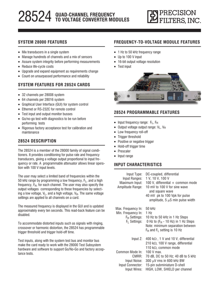
28524 QUAD-CHANNEL FREQUENCY TO VOLTAGE CONVERTER MODULES SYSTEM 28000 FEATURES FREQUENCY-TO-VOLTAGE MODULE FEATURES · · · · · · · · · · Mix transducers in a single system Manage hundreds of channels and a mix of sensors Assure system integrity before performing measurements Reduce life-cycle costs Upgrade and expand equipment as requirements change Count on unsurpassed performance and reliability 1 Hz to 50 kHz frequency range Up to 100 V input 16-bit output voltage resolution Test input SYSTEM FEATURES FOR 28524 CARDS · · · · · · 32 channels per 28008 system 64 channels per 28016 system Graphical User Interface (GUI) for system control Ethernet or RS-232C for remote control Test input and output monitor busses Go/no-go test with diagnostics to be run before performing tests · Rigorous factory acceptance test for calibration and maintenance 28524 DESCRIPTION The 28524 is a member of the 28000 family of signal conditioners. It provides conditioning for pulse rate and frequency transducers, giving a voltage output proportional to input frequency or rate. A programmable attenuator allows linear operation with 100 V input levels. The user may select a limited band of frequencies within the 50 kHz range by programming a low frequency, F L, and a high frequency, FH, for each channel. The user may also specify the output voltages corresponding to these frequencies by selecting a low voltage, VL, and a high voltage, VH. The same voltage settings are applied to all channels on a card. The measured frequency is displayed in the GUI and is updated approximately every ten seconds. This read-back feature can be disabled. To accommodate distorted inputs such as signals with ringing, crossover or harmonic distortion, the 28524 has programmable trigger threshold and trigger hold-off time. Test inputs, along with the system test bus and monitor bus make the card ready to work with the 28000 Test Subsystem hardware and software to support Go/No-Go and factory acceptance tests. 28524 PROGRAMMABLE FEATURES · · · · · · · · Input frequency range: FL, FH Output voltage output range: VL, VH Low frequency roll-off Trigger threshold Positive or negative trigger Hold-off trigger time Prescaler Input range INPUT CHARACTERISTICS Input Type: Input Ranges: Maximum Input: Amplitude Range: DC-coupled, differential 1 V, 10 V, 100 V 100 V, differential + common mode 10 mV to 100 V for sine wave and square wave 40 mV pk to 100 Vpk for pulse amplitude, 5 mS min pulse width Max. Frequency In: 50 kHz Min. Frequency In: 1 Hz FH Settings: 10 Hz to 50 kHz in 1 Hz Steps FL Settings: 0 Hz to (FH - 10 Hz) in 1 Hz Steps Note: minimum separation between FH and FL setting is 10 Hz Input Z: 400 kW , 1 V and 10 V, differential 210 kW, 100 V range, differential 110 kW, common mode Common Mode In: 100 V max. CMRR: 70 dB, DC to 50 Hz; 40 dB to 5 kHz Input Noise: 300 mV rms in 600 kHz BW Input Connector: 15-pin subminiature D-shell Input Wires: HIGH, LOW, SHIELD per channel 28524 TRIGGER TRIGGER (Continued) Selectable Trigger Type Programmable Trigger Threshold Positive or negative edge trigger, user selectable. The programmable trigger threshold allows the user to adjust the trigger voltage up or down to avoid distorted portions of the input signal. A signal with crossover distortion could cause false triggering. See Figure 3. The selectable edge trigger allows the user to choose the positive (leading) or negative (trailing) signal edge. Selecting the edge with the sharper transition produces a more stable output. See Figure 1. Trigger Threshold 100V range: ± 100 V in 50 mV steps 10V range: ± 10 V in 5 mV steps 1V range: ± 1 V in 500 µV steps Trigger Threshold Trigger Positive Trigger Trigger Trigger Jitter Negative Trigger Trigger Trigger Figure 1 Selectable Trigger The programmable trigger hold-off time prevents false triggering on signal edges which cross the trigger threshold voltage but are not representative of the actual input frequency. On each valid edge, the trigger circuit is disabled for a period of time to ignore the false edges. An input signal with ringing could cause false triggering. See Figure 2. Range: 1 mS to 1 S in 1 mS steps Trigger Trigger Trigger Converter Sees Trigger Threshold Adjusted Up Trigger Converter Sees Programmable Trigger Hold Off Period Trigger Figure 3 Programmable Trigger Threshold Auto Trigger When initiated, the system automatically determines a trigger threshold for a stable input waveform. PRESCALER The programmable prescaler divides the input signal by 2 to 255 by counting the specified number of input edges before passing a trigger pulse to the converter circuitry. Trigger Threshold In a system where the signal is generated by a transducer sensing gear teeth or flow meter vanes, the signal can be scaled to volts/revolution by dividing the input by the number of teeth or vanes. Without Hold Off With Hold Off Hold Off Period Hold Off Period Figure 2 Programmable Trigger Hold Off Page 2 Input Signal 28524 INPUT FILTERS 28524 OUTPUT CHARACTERISTICS (Cont.) The 28524 provides programmable cascaded high-pass and low-pass filters at the input. Freq. Measurement Accuracy: ±0.03% typical High-Pass Filters: 1-pole; 10 Hz, 100 Hz, or Bypass Low-Pass Filters: 4-pole Bessel Precision Filters, A range: 5 Hz to 1.275 kHz in 5 Hz steps (low), 1.5 kHz to 127.5 kHz in 500 Hz steps (high). FC is slaved to the upper input frequency setting such that: FC = 5*FH for FH £ 25.5 kHz and FC = 127.5 kHz for FH > 25 .5 kHz. The low-pass filter can be bypassed. 28524 OUTPUT CHARACTERISTICS Max. Voltage Out: ±10 VDC VH Settings: -9 V to 10 V in 0.1 V steps VL Settings: –10 V to (VH -1 V) in 0.1 V steps Type: DC coupled, single-ended output with Ground sense Output Filter Type: 2-pole Bessel Output Filter Fc’s: 1 Hz, 10 Hz, 100 Hz, Bypass Z: 50 W || 100 pF Voltage Output Resolution: (FH - FL)/65535 Hz Initial Accuracy: ±2 mV ±0.01% (VH - VL) ±0.015%*e accuracy typical ±5 mV ±0.05% (VH - VL) ±0.015%*e accuracy, max Where e = FH /(FH - FL) Drift: (100 ppm of setting + 20 mV)/°C Noise: 100 mV ÖHz, 1 MHz BW Pulse Output: 5 V CMOS, FOUT = FIN Freq. Display Resolution: 1.00 to 999.99 in 0.01 Hz steps 1,000.0 to 9,999.9 in 0.1 Hz steps 10,000 to 50,000 in 1 Hz steps Rear Output Conns: 26-pin D-shell for VDC and pulse out 50-pin D-Shell for VDC Front Output Conns: 48-pin DIN for pulse outputs TRANSFER CHARACTERISTICS VDC Output Update Rate: Fin > 1kHz: 1 to 2 mS Fin < 1kHz: 1/Fin S + 1 mS Settling time to 0.05% of final value: Output Filter Bypassed: @125 mS Output Filter Fc = 1 Hz: 1.2 S Output Filter Fc =10 Hz: 120 mS Output Filter Fc =100 Hz: 12 mS Pulse output: 5V square wave, FOUT = FIN TEST BUS A switch at the input of each channel allows the application of a signal for test and calibration. The test bus is used by the Test Subsystem module. Also, an input can be simulated via GUI control. The user enters a frequency and the 28524 loads the output DAC with the appropriate value taking into account the FH, FL, VH, and VL set points. Frequency Entry Resolution: 1.00 to 999.99 in 0.01 Hz steps 1,000.0 to 9,999.9 in 0.1 Hz steps 10,000 to 50,000 in 1 Hz steps Monitor Bus Gain/Atten. Buffer High-Pass Low-Pass Filters Input Monitor Bus Trigger Offset Pulse Out Monitor Bus Test Bus Edge Selection Hold-Off Prescaling Conversion Output Span Offset Figure 4 Block Diagram of Typical 28524 Channel Output Filter VDC Output Page 3 MONITOR BUS ACCESSORIES Switches at the trigger level input circuit, conversion output and pulse output allow for connection to the output monitor bus. The output monitor bus is available via BNC at the mainframe front panel. The monitor bus is used by the Test Subsystem module. Mating Connectors Precision Filters mating connectors accommodate up to 22 AWG wire and are supplied with high quality metal backshells and gold plated screw machined contacts for high reliability connections and long service life. CHARACTERISTICS 28524 Card Size: 6.63 x 17.5 x 0.75 inches Card Weight: 1.3 lbs net, 3 lbs shipping Temperature: 0o to 40o C (operating) –20o to 70o C (storage) CONN-IN-15D: Multipin 15-pin D-shell mating input connector with crimp sockets and metal backshell with strain relief. CONN-IN-15D-SC: Multipin 15-pin D-shell mating input connector with solder cup sockets and metal backshell with strain relief. CONN-OUT-26D-MTL: High-Density 26-pin D-shell mating output connector with machined solder cup pins and metal backshell with strain relief with large hole. CONN-OUT-26D-SC-MTL: High-Density 26-pin D-shell mating output connector with machined solder cup pins and metal backshell with strain relief with large hole. Output Adapter 28524 cards are fitted with front panel connectors that accept the output adapter modules in order to provide multiple buffered “pulse” outputs. Adapters plug on to the front of the signal conditioner card and are secured to the card by two screws. The adapters provide four additional fully buffered BNC outputs per channel and one 15-pin D-shell output connector. 28524 Input and Output Connectors The BUFF-4BNC/15D Quad output buffer module provides one buffered output per channel on 4 BNC connectors or one 15-pin multipin connector. BUFF-4CH/(2)15C: Quad output buffer with dual outputs per channel on two 15-pin connectors. P 8383 Rev B


