2015-12-23
Silicon PIN Photodiode
Version 1.3
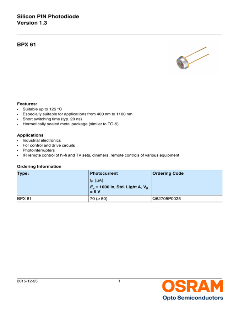
BPX 61
Features:
•
Suitable up to 125 °C
•
Especially suitable for applications from 400 nm to 1100 nm
•
Short switching time (typ. 20 ns)
•
Hermetically sealed metal package (similar to TO-5)
Applications
Industrial electronics
•
•
For control and drive circuits
•
Photointerrupters
•
IR remote control of hi-fi and TV sets, dimmers, remote controls of various equipment
Ordering Information
Type:
Photocurrent
Ordering Code
IP [µA]
Ev = 1000 lx, Std. Light A, VR
=5V
BPX 61
2015-12-23
70 (≥ 50)
Q62705P0025
1
Version 1.3
BPX 61
Maximum Ratings (TA = 25 °C)
Parameter
Symbol
Values
Unit
Operating and storage temperature range
Top; Tstg
-40 ... 125
°C
Reverse voltage
VR
32
V
Total Power dissipation
Ptot
250
mW
ESD withstand voltage
(acc. to ANSI/ ESDA/ JEDEC JS-001 - HBM)
VESD
2000
V
Characteristics (TA = 25 °C)
Parameter
Symbol
Values
Unit
Spectral sensitivity
(VR = 5 V)
(typ)
S
70 (≥ 50)
nA/Ix
Photocurrent
(Ev = 1000 lx, Std. Light A, VR = 5 V)
(typ (min))
IP
70 (≥ 50)
µA
Wavelength of max. sensitivity
(typ)
λS max
850
nm
Spectral range of sensitivity
(typ)
λ10%
Radiant sensitive area
(typ)
A
Dimensions of radiant sensitive area
(typ)
LxW
Half angle
(typ)
ϕ
Dark current
(VR = 10 V)
(typ (max)) IR
Spectral sensitivity of the chip
(λ = 850 nm)
(typ)
Sλ typ
0.62
A/W
Quantum yield of the chip
(λ = 850 nm)
(typ)
η
0.90
Electro
ns
/Photon
Open-circuit voltage
(Ev = 1000 lx, Std. Light A)
(typ (min))
VO
375 (≥ 320)
mV
Short-circuit current
(Ev = 1000 lx, Std. Light A)
(typ)
ISC
70
µA
Rise and fall time
(VR = 5 V, RL = 50 Ω, λ = 850 nm, IP = 800 µA)
(typ)
tr, tf
0.02
µs
Forward voltage
(IF = 100 mA, E = 0)
(typ)
VF
1.3
V
Capacitance
(VR = 0 V, f = 1 MHz, E = 0)
(typ)
C0
72
pF
Temperature coefficient of VO
(typ)
TCV
2015-12-23
2
(typ) 400
... 1100
nm
7.02
mm2
2.65 x 2.65
mm x
mm
± 55
2 (≤ 30)
-2.6
°
nA
mV / K
Version 1.3
BPX 61
Parameter
Symbol
Values
Unit
Temperature coefficient of ISC
(Std. Light A)
(typ)
TCI
0.18
%/K
Noise equivalent power
(VR = 10 V, λ = 850 nm)
(typ)
NEP
0.041
pW /
Hz½
Detection limit
(typ)
D*
6.5e12
cm x
Hz½ / W
Relative Spectral Sensitivity 1) page 7
Srel = f(λ)
100
Photocurrent / Open-Circuit Voltage 1) page 7
IP (VR = 5 V) / VO = f(EV)
OHF00078
S rel %
80
60
40
20
0
400 500 600 700 800 900 nm 1100
λ
2015-12-23
3
Version 1.3
BPX 61
Dark Current 1) page 7
IR = f(VR), E = 0
Power Consumption
Ptot = f(TA)
OHF00080
4000
ΙR
pA
3000
2000
1000
0
Capacitance 1) page 7
C = f(VR), f = 1 MHz, E = 0
5
10
15
V
VR
20
Dark Current 1) page 7
IR = f(TA), VR = 10 V, E = 0
OHF00081
100
C
0
OHF00082
10 3
Ι R nA
pF
80
10 2
70
60
10 1
50
40
30
10 0
20
10
0 -2
10
10 -1
10 0
10 1
10 -1
V 10 2
VR
2015-12-23
4
0
20
40
60
80 ˚C 100
TA
Version 1.3
BPX 61
Directional Characteristics 1) page 7
Srel = f(ϕ)
Package Outline
Cathode
ø0.45 (0.018)
3.4 (0.134)
14.5 (0.571)
3.0 (0.118)
12.5 (0.492)
0.3 (0.012) max
Approx. weight 2 g
0.8
0.6 5 (0
5 ( .03
0.0 3)
26
)
9)
.0 03 1)
(
3
1.0 (0.0
0.8
GMOY6011
Dimensions in mm (inch).
Package
Metal Can (TO-39), hermetically sealed
2015-12-23
Radiant
sensitive area
ø5.8 (0.228)
1.55 (0.061)
ø6.0 (0.236)
1.75 (0.069)
5.08 (0.200)
spacing
ø9.5 (0.374)
ø9.0 (0.354)
ø8.3 (0.327)
ø8.0 (0.315)
Chip position
5
Version 1.3
BPX 61
Approximate Weight:
0.9 g
TTW Soldering
IEC-61760-1 TTW
OHA04645
300
10 s max., max. contact time 5 s per wave
˚C
T 250
235 ˚C - 260 ˚C
First wave
Second wave
Continuous line: typical process
Dotted line: process limits
∆T < 150 K
200
Cooling
Preheating
ca. 3.5 K/s typical
150
ca. 2 K/s
130 ˚C
120 ˚C
100 ˚C
100
ca. 5 K/s
Typical
50
0
0
20
40
60
80
100
120
140
160
180
200
220 s 240
t
Disclaimer
Language english will prevail in case of any discrepancies or deviations between the two language wordings.
Attention please!
The information describes the type of component and shall not be considered as assured characteristics.
Terms of delivery and rights to change design reserved. Due to technical requirements components may contain
dangerous substances.
For information on the types in question please contact our Sales Organization.
If printed or downloaded, please find the latest version in the Internet.
Packing
Please use the recycling operators known to you. We can also help you – get in touch with your nearest sales office.
By agreement we will take packing material back, if it is sorted. You must bear the costs of transport. For packing
material that is returned to us unsorted or which we are not obliged to accept, we shall have to invoice you for any
costs incurred.
Components used in life-support devices or systems must be expressly authorized for such purpose!
Critical components* may only be used in life-support devices** or systems with the express written approval of
OSRAM OS.
*) A critical component is a component used in a life-support device or system whose failure can reasonably be
expected to cause the failure of that life-support device or system, or to affect its safety or the effectiveness of that
device or system.
**) Life support devices or systems are intended (a) to be implanted in the human body, or (b) to support and/or
maintain and sustain human life. If they fail, it is reasonable to assume that the health and the life of the user may be
endangered.
2015-12-23
6
Version 1.3
BPX 61
Glossary
1)
Typical Values: Due to the special conditions of the manufacturing processes of LED, the typical data or
calculated correlations of technical parameters can only reflect statistical figures. These do not necessarily
correspond to the actual parameters of each single product, which could differ from the typical data and calculated
correlations or the typical characteristic line. If requested, e.g. because of technical improvements, these typ. data
will be changed without any further notice.
2015-12-23
7
Version 1.3
BPX 61
Published by OSRAM Opto Semiconductors GmbH
Leibnizstraße 4, D-93055 Regensburg
www.osram-os.com © All Rights Reserved.
2015-12-23
8
