CIRCUIT FUNCTION AND BENEFITS
1
NC
2
GND
3
VIN
ADR127
VDD
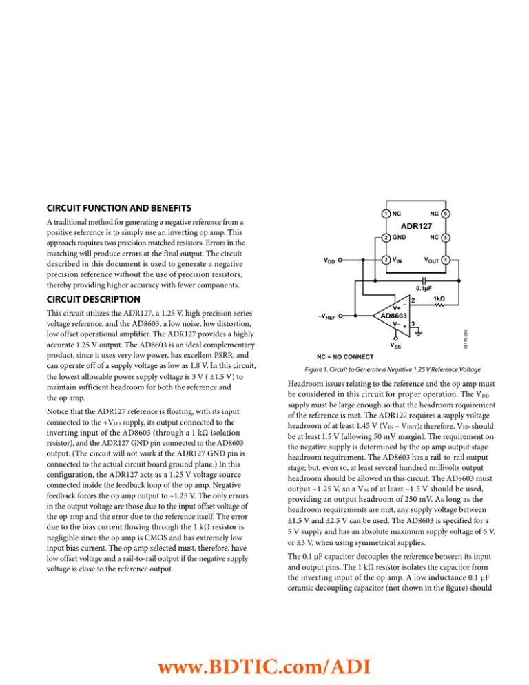
Notice that the ADR127 reference is floating, with its input
connected to the +VDD supply, its output connected to the
inverting input of the AD8603 (through a 1 kΩ isolation
resistor), and the ADR127 GND pin connected to the AD8603
output. (The circuit will not work if the ADR127 GND pin is
connected to the actual circuit board ground plane.) In this
configuration, the ADR127 acts as a 1.25 V voltage source
connected inside the feedback loop of the op amp. Negative
feedback forces the op amp output to –1.25 V. The only errors
in the output voltage are those due to the input offset voltage of
the op amp and the error due to the reference itself. The error
due to the bias current flowing through the 1 kΩ resistor is
negligible since the op amp is CMOS and has extremely low
input bias current. The op amp selected must, therefore, have
low offset voltage and a rail-to-rail output if the negative supply
voltage is close to the reference output.
NC 5
VOUT 4
0.1µF
CIRCUIT DESCRIPTION
This circuit utilizes the ADR127, a 1.25 V, high precision series
voltage reference, and the AD8603, a low noise, low distortion,
low offset operational amplifier. The ADR127 provides a highly
accurate 1.25 V output. The AD8603 is an ideal complementary
product, since it uses very low power, has excellent PSRR, and
can operate off of a supply voltage as low as 1.8 V. In this circuit,
the lowest allowable power supply voltage is 3 V ( ±1.5 V) to
maintain sufficient headroom for both the reference and
the op amp.
NC 6
V+
–VREF
–
2
1kΩ
AD8603
V– + 3
VSS
08176-055
A traditional method for generating a negative reference from a
positive reference is to simply use an inverting op amp. This
approach requires two precision matched resistors. Errors in the
matching will produce errors at the final output. The circuit
described in this document is used to generate a negative
precision reference without the use of precision resistors,
thereby providing higher accuracy with fewer components.
NC = NO CONNECT
Figure 1. Circuit to Generate a Negative 1.25 V Reference Voltage
Headroom issues relating to the reference and the op amp must
be considered in this circuit for proper operation. The VDD
supply must be large enough so that the headroom requirement
of the reference is met. The ADR127 requires a supply voltage
headroom of at least 1.45 V (VIN – VOUT); therefore, VDD should
be at least 1.5 V (allowing 50 mV margin). The requirement on
the negative supply is determined by the op amp output stage
headroom requirement. The AD8603 has a rail-to-rail output
stage; but, even so, at least several hundred millivolts output
headroom should be allowed in this circuit. The AD8603 must
output –1.25 V, so a V SS of at least –1.5 V should be used,
providing an output headroom of 250 mV. As long as the
headroom requirements are met, any supply voltage between
±1.5 V and ±2.5 V can be used. The AD8603 is specified for a
5 V supply and has an absolute maximum supply voltage of 6 V,
or ±3 V, when using symmetrical supplies.
The 0.1 µF capacitor decouples the reference between its input
and output pins. The 1 kΩ resistor isolates the capacitor from
the inverting input of the op amp. A low inductance 0.1 µF
ceramic decoupling capacitor (not shown in the figure) should
www.BDTIC.com/ADI
be connected to VDD very close to the two ICs. In most cases,
the final output of the op amp (–VREF) will be heavily decoupled,
which means that the op amp selected must be stable with large
capacitive loads. A typical decoupling network consists of a 1 µF
to 10 µF electrolytic capacitor in parallel with a 0.1 µF low
inductance ceramic MLCC type.
COMMON VARIATIONS
The circuit is proven to work with good stability and accuracy
with component values shown. Other ADI voltage references
and precision op amps can be used in this configuration to
develop negative references with other desired values.
When selecting reference and amplifier combinations, always
ensure that the Supply Voltage Headroom specification
(VIN – VOUT) of the reference is not violated. Since the reference
VOUT = 0, the minimum value of +VDD must be equal to or
greater than the Supply Voltage Headroom. For example, to
generate a –5 V reference using the ADR365 precision 5 V
reference, we need a +VDD of at least 5.3 V, since the Supply
Voltage Headroom specification of the ADR365 is 300 mV.
The amplifier must supply a negative 5 V at its output, so in
this case a good choice for the amplifier would be the AD8663
16 V, low noise, precision, rail-to-rail op amp. VSS should be set
at –5.5 V (to allow 0.5 V negative output headroom), and VDD
can range anywhere from 5.3 V to 10.5 V, due to the 16 V
supply range of the AD8663. In most cases the supplies are
symmetrical, so VDD = +5.5 V and VSS = –5.5 V would be
good choices.
The ADR121 can be used with an appropriate op amp to
generate a –2.5 V reference. Since the op amp must output a
voltage of –2.5 V, a V SS of at least –2.8 V should be used
(assuming a rail-to-rail output stage). VDD must be at least
+0.3 V to meet the minimum VIN – VOUT requirement of the
ADR121. If the AD8603 is used, VDD should be no higher than
+2.2 V so that the total supply voltage across the AD8603 is no
greater than 5 V. If symmetrical 2.8 V supplies or higher are
required (±5 V, for example), an op amp with a higher supply
voltage must be chosen.
LEARN MORE
Jung, Walter G. 2002. Op Amp Applications. Analog Devices.
ISBN 0916550265. Chapter 7. Also available as Op Amp
Applications Handbook. Elsevier/Newnes. 2005. ISBN
0750678445. Chapter 7, http://www.analog.com/library/
analogDialogue/archives/39-05/op_amp_applications_
handbook.html.
Kester, Walt. 2004. Analog-Digital Conversion. Analog Devices.
ISBN 0916550273. Chapter 9. Also available as The Data
Conversion Handbook. Elsevier/Newnes. 2005. ISBN
0750678410, Chapter 9, http://www.analog.com/library/
analogDialogue/archives/39-6/data_ conversion_
handbook.html.
Zumbahlen, Hank. 2006. Basic Linear Design. Analog Devices.
ISBN 0915550281. Chapter 11. Also available as Linear
Circuit Design Handbook. Elsevier-Newnes, 2008, ISBN
0750687037, Chapter 11, http://www.elsevierdirect.com/
product.jsp?isbn=9780750687034&ref=CWS1.
Data Sheets
ADR127 Data Sheet. http://www.analog.com/en/ADR127/
productsearch.html.
AD8603 Data Sheet. http://www.analog.com/en/AD8603/
productsearch.html.
REVISION HISTORY
4/09—Rev. 0 to Rev. A
Updated Format .................................................................. Universal
10/08—Revision 0: Initial Version
(Continued from first page) "Circuits from the Lab" are intended only for use with Analog Devices products and are the intellectual property of Analog Devices or its licensors. While you may
use the "Circuits from the Lab" in the design of your product, no other license is granted by implication or otherwise under any patents or other intellectual property by application or use of
the "Circuits from the Lab". Information furnished by Analog Devices is believed to be accurate and reliable. However, "Circuits from the Lab" are supplied "as is" and without warranties of any
kind, express, implied, or statutory including, but not limited to, any implied warranty of merchantability, noninfringement or fitness for a particular purpose and no responsibility is assumed
by Analog Devices for their use, nor for any infringements of patents or other rights of third parties that may result from their use. Analog Devices reserves the right to change any "Circuits
from the Lab" at any time without notice, but is under no obligation to do so. Trademarks and registered trademarks are the property of their respective owners.
©2008–2009 Analog Devices, Inc. All rights reserved. Trademarks and
registered trademarks are the property of their respective owners.
CN08176-0-4/09(A)
www.BDTIC.com/ADI


