Regular Question Papers
advertisement
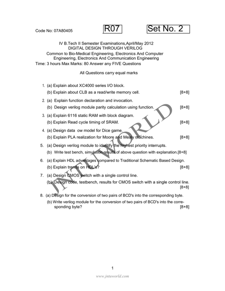
R07 Code No: 07A80405 Set No. 2 IV B.Tech II Semester Examinations,April/May 2012 DIGITAL DESIGN THROUGH VERILOG Common to Bio-Medical Engineering, Electronics And Computer Engineering, Electronics And Communication Engineering Time: 3 hours Max Marks: 80 Answer any FIVE Questions All Questions carry equal marks 1. (a) Explain about XC4000 series I/O block. (b) Explain about CLB as a read/write memory cell. [8+8] 2. (a) Explain function declaration and invocation. (b) Design verilog module parity calculation using function. [8+8] 3. (a) Explain 6116 static RAM with block diagram. (b) Explain Read cycle timing of SRAM. [8+8] 4. (a) Design data ow model for Dice game. (b) Explain PLA realization for Moore and Mealy machines. [8+8] 5. (a) Design verilog module to identify the highest priority interrupts. (b) Write test bench, simulation results of above question with explanation.[8+8] 6. (a) Explain HDL advantages compared to Traditional Schematic Based Design. (b) Explain trends on HDL's? [8+8] 7. (a) Design CMOS switch with a single control line. (b) Design code, testbench, results for CMOS switch with a single control line. [8+8] 8. (a) Design for the conversion of two pairs of BCD's into the corresponding byte. (b) Write verilog module for the conversion of two pairs of BCD's into the corresponding byte? [8+8] 1 www.jntuworld.com Code No: 07A80405 R07 Set No. 4 IV B.Tech II Semester Examinations,April/May 2012 DIGITAL DESIGN THROUGH VERILOG Common to Bio-Medical Engineering, Electronics And Computer Engineering, Electronics And Communication Engineering Time: 3 hours Max Marks: 80 Answer any FIVE Questions All Questions carry equal marks 1. (a) Explain memory Controller SM Chart for Read cycle. (b) Explain and Draw Chip select timing for Write to RAM. [8+8] 2. (a) Explain SM chart for binary multiplier. (b) Write HDL code for the binary multiplier. [8+8] 3. (a) Classify and explain strengths and contention resolution. (b) Design a module to illustrate use of the wand-type net and test bench with stimulation results? [8+8] 4. (a) Explain NMOS enhancement with conditions. (b) Write about Basic switch primitives. 5. Design behavioral model of HDL XC4000 CLB. [8+8] [16] 6. (a) Explain the Pin-to-Pin Delay with example. (b) Explain and specify blocks of Path Delay Modeling. [8+8] 7. De ne a task to compute the factorial of a 4 bit number.The output is a 32 bit value.The result is assigned to the output after a delay of 10 time units. [16] 8. (a) Design a Module to add two pairs of BCD nibbles (2 decimal no's each of two digit). (b) Write a verilog code to add two pairs of BCD nibbles (2 decimal no's each of [8+8] two digit). 2 Code No: 07A80405 R07 Set No. 1 IV B.Tech II Semester Examinations,April/May 2012 DIGITAL DESIGN THROUGH VERILOG Common to Bio-Medical Engineering, Electronics And Computer Engineering, Electronics And Communication Engineering Time: 3 hours Max Marks: 80 Answer any FIVE Questions All Questions carry equal marks 1. (a) Design SM chart for Dice game test. (b) Write Tester for Dice game (HDL module). [8+8] 2. (a) Explain micro processor Bus Interface. (b) Explain Intel 486 basic 3-3 Bus cycle. [8+8] 3. (a) Design a JK ip op using NAND gates. (b) Write a verilog code for JK ip op using NAND gates. 4. Explain signal paths within adder subtractor logic cell. [8+8] [16] 5. (a) Write about $ readmemb with example. (b) Write value change dump le. [8+8] 6. (a) Design verilog code of OR gate using for and disable. (b) Write simulation results of above question with explanation. [8+8] 7. (a) Design basic functional unit of a dynamic shift register. (b) Write the verilog code for basic functional unit of a dynamic shift register. [8+8] 8. Explain bottom up design methodology with example? 3 [16] Code No: 07A80405 R07 Set No. 3 IV B.Tech II Semester Examinations,April/May 2012 DIGITAL DESIGN THROUGH VERILOG Common to Bio-Medical Engineering, Electronics And Computer Engineering, Electronics And Communication Engineering Time: 3 hours Max Marks: 80 Answer any FIVE Questions All Questions carry equal marks 1. (a) Explain the SM chart with: i. parallel form ii. serial form. (b) Explain the conversion of a state graph to an SM chart. [8+8] 2. Explain about Programmable interconnects-XC4000. [16] 3. Explain the following "lexical conventions" with examples. (a) White space (b) Comments [16] (c) Operators 4. (a) Explain with any one example fork-join block within a begin-end block. (b) Write any one example of a begin-end block with in a fork-join block. [8+8] 5. Write HDL model for 486 Bus Interface Unit. [16] 6. (a) Design a skeletal edge-triggered ip op. (b) Write verilog module for a positive edge triggered ip op with test bench. [8+8] 7. (a) Explain hierarchy of the blocks and module instantiation. (b) Design verilog module for hierarchy of the blocks and module instantiation with example. [8+8] 8. (a) Design CMOS switch of parallel combination. (b) Write the code for CMOS switch of parallel combination. [8+8]
