The CMOS Inverter: Current Flow during Switching A B D E C
advertisement
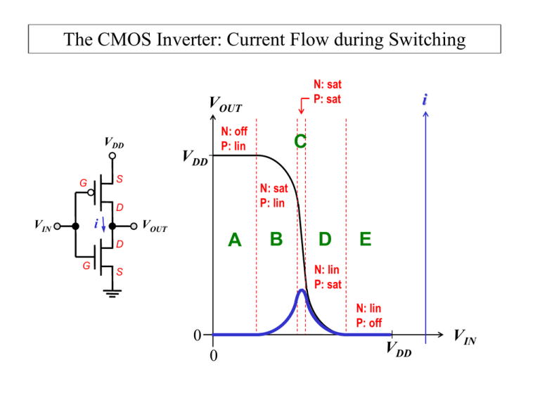
EECS 40 Fall 2001 Lecture 2 W. G. Oldham Copyright Regents of University of California The CMOS Inverter: Current Flow during Switching N: sat P: sat VOUT N: off P: lin VDD VDD S G i VOUT A D G C N: sat P: lin D VIN i B D E N: lin P: sat S N: lin P: off 0 0 VDD VIN EECS 40 Fall 2001 Lecture 2 W. G. Oldham Copyright Regents of University of California Power Dissipation due to Direct-Path Current VDD VDD vIN: S G D i vIN S VT 0 Ipeak vOUT D G VDD-VT i: 0 tsc Energy consumed per switching period: time Edp = t scVDD I peak EECS 40 Fall 2001 Lecture 2 W. G. Oldham Copyright Regents of University of California N-Channel MOSFET Operation An NMOSFET is a closed switch when the input is high A A B B Y X Y X Y = X if A and B Y = X if A or B NMOSFETs pass a “strong” 0 but a “weak” 1 EECS 40 Fall 2001 Lecture 2 W. G. Oldham Copyright Regents of University of California P-Channel MOSFET Operation A PMOSFET is a closed switch when the input is low A A B B Y X Y = X if A and B = (A + B) Y X Y = X if A or B = (AB) PMOSFETs pass a “strong” 1 but a “weak” 0 EECS 40 Fall 2001 Lecture 2 W. G. Oldham Copyright Regents of University of California Pull-Down and Pull-Up Devices • In CMOS logic gates, NMOSFETs are used to connect the output to GND, whereas PMOSFETs are used to connect the output to VDD. – An NMOSFET functions as a pull-down device when it is turned on (gate voltage = VDD) – A PMOSFET functions as a pull-up device when it is turned on (gate voltage = GND) VDD Pull-up network PMOSFETs only F(A1, A2, …, AN) … A1 A2 AN … input signals A1 A2 AN Pull-down network NMOSFETs only EECS 40 Fall 2001 Lecture 2 Copyright Regents of University of California W. G. Oldham CMOS NAND Gate VDD A A B 0 0 0 1 1 0 1 1 B F A B F 1 1 1 0 EECS 40 Fall 2001 Lecture 2 Copyright Regents of University of California W. G. Oldham CMOS NOR Gate VDD A B 0 0 0 1 1 0 1 1 A B F B A F 1 0 0 0 EECS 40 Fall 2001 Lecture 2 W. G. Oldham Copyright Regents of University of California CMOS Pass Gate A Y X A Y = X if A EECS 40 Fall 2001 Lecture 2 W. G. Oldham Copyright Regents of University of California Logic Gates – From Week 9b A A AND F=A·B B B A B A B F=A+B OR A A NOT A B NAND F = A⋅ B NOR F = A+ B F = A⊕B EXCLUSIVE OR EECS 40 Fall 2001 Lecture 2 Copyright Regents of University of California W. G. Oldham Logic Gates – How are they used? A AND C=A·B B First of all we must agree on what is high (logical 1) or low (logical 0). Suppose 1.5 V is 1 and 0V is logical 0. + AND 1.5V + 1.5V - C would have the value of 1.5 V (logical 1). But it would have the value of 0V (logical 0) if either one of the inputs were held at zero V. EECS 40 Fall 2001 Lecture 2 W. G. Oldham Copyright Regents of University of California What are the most basic gates in Digital Electronics? Not-AND = NAND A AB B Not-OR = NOR A B A+ B A 0 0 1 1 B 0 1 0 1 AB AB 0 1 0 1 0 1 1 0 A 0 0 1 1 B 0 1 0 1 A+B A + B 0 1 1 1 1 0 0 0 Typically use one or the other: “NAND logic” or “NOR logic” EECS 40 Fall 2001 Lecture 2 W. G. Oldham Copyright Regents of University of California How to Combine Gate to Produce a Desired Logic Function? (This is called Logical Synthesis) le p am x E Not-AND = NAND Logically just an AND plus a NOT gate: A AB B A B AND AB NOT Shor A B AND AB OT N r o f thand EECS 40 Fall 2001 Lecture 2 W. G. Oldham Copyright Regents of University of California How to Combine Gate to Produce a Desired Logic Function? (More basic Logical Synthesis) F= A . B le p am x E A AB B Again a little shorthand is useful A B A .B EECS 40 Fall 2001 Lecture 2 Copyright Regents of University of California W. G. Oldham How to Combine Gate to Produce a Desired Logic Function? (More basic Logical Synthesis) Suppose we are given a truth table (all logic statements can be represented by a truth table). How can we implement the function? Answer: There are lots of ways, but one simple way is implementation from “sum of products” formulation. How to do this: 1) Write sum of products expression from truth table and 2) Implement using standard gates. (Warning this is probably inefficient – we need to minimize, or simplify the expression) EECS 40 Fall 2001 Lecture 2 W. G. Oldham Copyright Regents of University of California How to Combine Gate to Produce a Desired Logic Function? (More basic Logical Synthesis) Example: Clearly: F= 1 if A B C F 0 0 0 0 0 0 1 1 0 1 0 0 0 1 1 0 1 0 0 0 1 0 1 0 1 1 0 1 1 1 1 0 ABC=1 or ABC =1 i.e. F= A B C +AB C EECS 40 Fall 2001 Lecture 2 Copyright Regents of University of California W. G. Oldham How to Combine Gate to Produce a Desired Logic Function? (More basic Logical Synthesis) Example: A B C F 0 0 0 0 0 0 1 1 0 1 0 0 0 1 1 0 1 0 0 0 1 0 1 0 1 1 0 1 1 1 1 0 F= A B C +AB C A B C A B C F EECS 40 Fall 2001 Lecture 2 W. G. Oldham Copyright Regents of University of California More Logical Synthesis Example: Thus A B F 0 0 0 A 0 1 1 B 1 0 0 1 1 1 F A B Clearly F=A B +AB But it is easy to show that a simpler valid expression for F is F = B , hence: B (ignore A) F EECS 40 Fall 2001 Lecture 2 Copyright Regents of University of California What circuit of logic gates could produce these (arbitrarily chosen) outputs F in response to inputs A, B and C? A 0 0 0 0 1 1 1 1 B 0 0 1 1 0 0 1 1 C 0 1 0 1 0 1 0 1 F 0 0 1 1 0 1 0 1 W. G. Oldham EECS 40 Fall 2001 Lecture 2 A B C A W. G. Oldham Copyright Regents of University of California A B C ABC ABC B F C ABC ABC Exam ple of general purpose circuit to implement the truth table of Table 22.4. (This solution is NOT minimized.) EECS 40 Fall 2001 Lecture 2 W. G. Oldham Copyright Regents of University of California Rules of boolean algebra. The two entries in the last row are used frequently and are known as DeMorgan’s theorem. AND Rules OR Rules A•A = A A+A = A A•A = 0 A+A = 1 0•A = 0 0+A = A 1•A = A 1+A = 1 A•B = B•A A+B = B+A A(BC) = (AB)C A+(B+C) = (A+B)+C A(B+C) = AB+AC A+BC = (A+B)(A+C) A•B A+B A+B A•B = = EECS 40 Fall 2001 Lecture 2 W. G. Oldham Copyright Regents of University of California Logical Synthesis Guided by DeMorgan’s Theorem Demorgan’s Theorem : [ A+B+C = A B C ] or A + B + C = [A B C] Thus, for example: F = AB + CD = AB • CD A B F C D Thus any sum of products expression can be immediately synthesized from NAND gates alone EECS 40 Fall 2001 Lecture 2 • W. G. Oldham Copyright Regents of University of California Karnaugh Maps Graphical approach to minimizing the number of terms in a logic expression: 1. 2. 3. 4. Map the truth table into a Karnaugh map (see below) For each 1, circle the biggest block that includes that 1 Write the product that corresponds to that block. Sum all of the products 4-variable Karnaugh Map 2-variable Karnaugh Map B 0 1 00 BC 00 01 11 10 0 1 A CD 00 01 11 10 3-variable Karnaugh Map 0 A 1 AB 01 11 10 EECS 40 Fall 2001 Lecture 2 W. G. Oldham Copyright Regents of University of California Karnaugh Map Example Input A 0 0 0 0 1 1 1 1 B 0 0 1 1 0 0 1 1 Output C 0 1 0 1 0 1 0 1 S1 0 0 0 1 0 1 1 1 S0 0 1 1 0 1 0 0 1 Simplification of expression for S1: BC A 0 00 01 11 10 0 0 1 0 1 0 BC 1 AC 1 AC 1 AB S1 = AB + BC + AC By simplifying we can reduce the number of gates, transistors, and the size of the circuits.
