ECN3296TF
advertisement

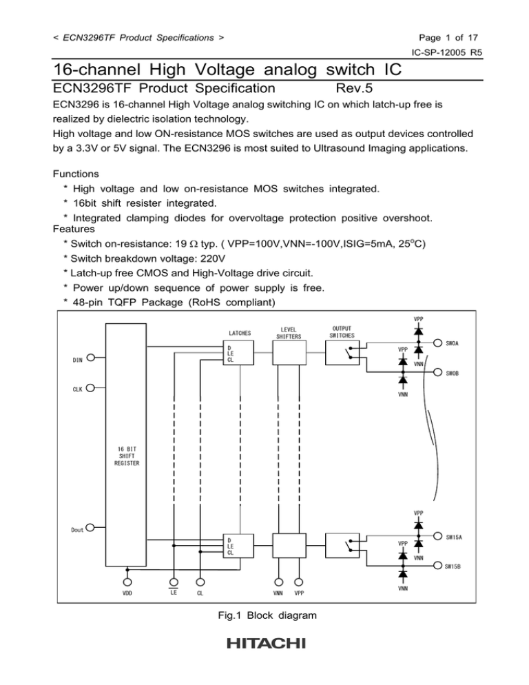
< ECN3296TF Product Specifications > Page 1 of 17 IC-SP-12005 R5 16-channel High Voltage analog switch IC ECN3296TF Product Specification Rev.5 ECN3296 is 16-channel High Voltage analog switching IC on which latch-up free is realized by dielectric isolation technology. High voltage and low ON-resistance MOS switches are used as output devices controlled by a 3.3V or 5V signal. The ECN3296 is most suited to Ultrasound Imaging applications. Functions * High voltage and low on-resistance MOS switches integrated. * 16bit shift resister integrated. * Integrated clamping diodes for overvoltage protection positive overshoot. Features * Switch on-resistance: 19 typ. ( VPP=100V,VNN=-100V,ISIG=5mA, 25oC) * Switch breakdown voltage: 220V * Latch-up free CMOS and High-Voltage drive circuit. * Power up/down sequence of power supply is free. * 48-pin TQFP Package (RoHS compliant) VPP LATCHES LEVEL SHIFTERS SW0A D LE CL DIN OUTPUT SWITCHES VPP VNN SW0B CLK VNN 16 BIT SHIFT REGISTER VPP Dout SW15A D LE CL VPP VNN SW15 B VDD LE CL VNN VPP Fig.1 Block diagram VNN < ECN3296TF Product Specifications > Page 2 of 17 IC-SP-12005 R5 1. General This Specification shall be applied to the following semiconductor integrated circuit. 1) 2) 3) 4) Parts name Application Structure Package : ECN3296TF : Ultrasound imaging scanner and others : Monolithic IC : TQFP48 2. Absolute Maximum Ratings Table 1 No. Absolute Maximum Ratings Items Symbol Terminal Values Unit Note VDD VDD -0.5 to +7.0 V Ta=25 C - VPP,VNN 220 V Ta=25 C o 1 Logic power supply voltage 2 VPP-VNN supply voltage 3 VPP Positive high voltage supply VPP VPP -0.5 to VNN+200 V Ta=25 C 4 VNN negative high voltage supply VNN VNN -200 to +0.5 V Ta=25 C 5 Logic input voltages VDD -0.5 to VDD+0.3 V Ta=25 C 6 Analog signal range SW0 to SW15 VNN to VPP V Ta=25 C 7 Operating junction temperature Tjop -20 to +125 o o DIN, CLK,CL, 8 Storage temperature Tstg -55 to +150 9 Power dissipation Pw 1.0 o o o o o C C W TQFP48 o Ta=70 C < ECN3296TF Product Specifications > Page 3 of 17 IC-SP-12005 R5 3. Electrical Characteristics 3.1 DC Characteristics Table 2 No. 1 Items Small signal switch on resistance o DC Characteristics Symbol RONS Ta=25 C Spec Unit Min Typ Max 24 17 19 15 19 15 38 27 27 24 25 25 VDD=5V Test conditions I SIG=5mA I SIG=200mA I SIG=5mA I SIG=200mA I SIG=5mA I SIG=200mA VPP=40V, VNN=-160V VPP=100V, VNN=-100V VPP=160V, VNN=-40V 2 Small signal switch on resistance matching ΔRONS 5 20 % 3 Large signal switch on resistance RONL 16 - 4 Switch off leakage per switch ISOL 1.0 10 A VSIG=VPP-10V, or VNN+10V 5 DC offset switch (off) DCOFF 10 100 mV RL=100kΩ 6 DC offset switch (on) DCON 10 100 mV RL=100kΩ 7 Positive HV supply current IPPQ1 10 50 A All SWs off INNQ1 -10 -50 A All SWs off IPPQ2 10 50 A All SWs on, ISW=5mA INNQ2 -10 -50 A All SWs on, ISW=5mA 7.0 7.0 8.0 7.0 7.0 8.0 8 Negative HV supply current 9 Positive HV supply current 10 Negative HV supply current 11 IPP Supply current 12 INN Supply current IPP INN mA mA VPP=100V, VNN=-100V ISW=5mA I SIG=1A VPP=100V VNN=-100V VPP=40V VNN=-160V VPP=100V VNN=-100V VPP=160V VNN=-40V VPP=40V VNN=-160V VPP=100V VNN=-100V VPP=160V VNN=-40V 50kHz output switching frequency without load 50kHz output switching frequency without load 13 Logic supply average current IDD 4.0 mA Logic supply quiescent current IDDQ 10 A 15 Data out source current ISOR 0.45 0.70 mA VOUT=VDD-0.7V 16 Data out sink current ISINK 0.45 0.70 mA VOUT=0.7V 14 fCLK=5MHz,VDD=5.0V < ECN3296TF Product Specifications > Page 4 of 17 IC-SP-12005 R5 3.2 AC Characteristics o Table 3 AC Characteristics No. Items Symbol Ta=25 C Spec Min Typ Max Unit VDD=5V Test conditions 1 SW Turn on time tON 5.0 s 2 SW Turn off time tOFF 5.0 s 30 3 Clock frequency fCLK 20 16 55 ns DOUT terminal,VDD=3.3V 12 42 ns DOUT terminal,VDD=5.0V +VSPK 150 Clock delay time to data out 4 5 Output voltage spike Table 4 No. Items Off capacitance SW to GND On Capacitance SW 2 to GND 1 3 SW off isolation 4 SW Crosstalk tDO -VSPK -150 +VSPK 150 -VSPK -150 +VSPK 150 -VSPK -150 VSIG=VPP-10V, RL=10kΩ VSIG=VPP-10V, RL=10kΩ 50% duty cycle, fData=fCLK/2 MHz VDD=5.0V 50% duty cycle, fData=fCLK/2 MHz VDD=3.3V VPP=40V, VNN=-160V, RL=50 mV VPP=100V, VNN=-100V, RL=50 VPP=160V, VNN=-40V, RL=50 AC Characteristics (for reference purpose only) Spec Symbol Unit Min Typ Max o Ta=25 C VDD=5V Condition CSG (off) 6 pF 0V, 1MHz CSG (on) 15 pF 0V, 1MHz -30 -33 dB fsw=5MHz, 1k//15pF load -54 -60 dB fsw=5MHz, 50 load -54 -60 dB fsw=5MHz, 50 load KO KCR Note: These items are not tested when shipped. < ECN3296TF Product Specifications > Page 5 of 17 IC-SP-12005 R5 4. Recommended Operating Conditions Please operate in use within the limit of recommended operating conditions detailed in Table 5. No Items Table 5 Recommended Operating Conditions Symbol Recommended Value 1 Logic power supply voltage VDD 3.0V to 5.5V 2 Positive high voltage supply VPP 40V to 160V 3 Negative high voltage supply VNN -160V to 0V 4 VPP-VNN supply voltage - 40V to 200V 5 High-level input voltage VIH 0.9VDD to VDD 6 Low-level input voltage VIL 0V to 0.1VDD 7 Analog signal voltage peak to peak VSIG VNN to VPP 8 9 Operating free air-temperature Ta Fsw 0 C to 70 C 50kHz max, Duty Cycle=50% Switching frequency o 10 Set up time for 11 Pulse width of TSD Min.60ns TWLE Min.40ns 12 Time width of CL TWCL Min.40ns 13 Set up time DATA to Clock TSU Min.10ns 14 Hold time DATA from Clock Th Min.10ns 15 Maximum VSIG Slew Rate dV/dt o Max.30V/ns Attention ; 1) Power up/down sequence of power supply is arbitrary except GND terminal of IC must be powered-up first and powered-down last. 2) It is indispensable to make there are not to exceed a maximum rated voltage by the occurrence of the excessive voltage in case of investing and cutting of the power supply. < ECN3296TF Product Specifications > Page 6 of 17 IC-SP-12005 R5 5. Test Circuit IC V PP-10V IC V PP-10V I SOL V OUT V NN+10V IC RL 10KΩ V OUT RL 100KΩ V PP V PP V DD 5V V PP V PP V DD 5V V PP V PP V DD 5V V NN V NN GND GND V NN V NN GND GND V NN V NN GND GND a) Switch OFF Leakage b) DC Offset ON/OFF IC V IN=10Vp-p @5MHz c) T ON/TOFF IC IC V IN=10Vp-p @5MHz V OUT +V spk V OUT ~ ~ 50Ω V OUT 50Ω -V spk NC 50Ω RL 1KΩ RL V PP V PP V DD 5V V PP V PP V DD 5V V PP V PP V DD 5V V NN V NN GND GND V NN V NN GND GND V NN V NN GND GND K o=20log(V OUT/V IN) d) Off Isolation K cr=20log(V OUT/V IN) e) Crosstalk Fig. 2 Test Circuit f) Output Voltage Spike < ECN3296TF Product Specifications > Page 7 of 17 IC-SP-12005 R5 6. Timing Waveforms DATA IN DN+1 DN 50% LE 50% tWLE 50% 50% tSD 50% CLOCK DN-1 tSU 50% th tDO DATA OUT 50% tOFF VOUT (typ) OFF 50% tON 90% 10% ON CLR tWCL Fig. 3 Timing Waveforms Note 1. Serial data is clocked in on the rising edge of CLK. 2. The switches go to a state retaining their present condition on the rising edge of tWLE LE tSD CLK tSU tW D15 DIN D14 D13 D1 MSB D0 LSB tDO DOUT D15 D14 D13 D1 Data from previous data byte ( power up : unknown ) Fig. 4 LATCH ENABLE Timing waveform D0 D15 . < ECN3296TF Product Specifications > Page 8 of 17 IC-SP-12005 R5 7Truth Table Table 6 Truth table D0 L H D1 D2 D3 D4 D5 D6 D7 L H L H L H L H L H L H X X X X D8 L H D9 L H X X X X X X X X X X X X X X L H X X LE L L L L L L L L L L L L L L L L H X D10 D11 D12 D13 D14 D15 LE L L L L L L H L L L H L L L H L L L H L L L H L L L H L X X X X X X H X X X X X X X CL SW0 SW1 SW2 SW3 SW4 SW5 SW6 SW7 L OFF L ON L OFF L ON L OFF L ON L OFF L ON L OFF L ON L OFF L ON L OFF L ON L OFF L ON HOLD PREVIOUS STATE L H OFF OFF OFF OFF OFF OFF OFF OFF CL SW8 SW9 SW10 SW11 SW12 SW13 L OFF L ON L OFF L ON L OFF L ON L OFF L ON L OFF L ON L OFF L ON L L L L HOLD PREVIOUS STATE L H OFF OFF OFF OFF OFF OFF X = Don’t care Note 1. The 16 Switches operate independently. 2. When is low, the shift register data flows through the latch. 3. Shift register clocking has no effect on the switch states if is high. 4. When switch 15 is ON, DOUT is high. 5. The clear input overrides all other inputs. SW14 SW15 OFF ON OFF ON OFF OFF < ECN3296TF Product Specifications > Page 9 of 17 IC-SP-12005 R5 8 Pin Configuration ECN3296TF TQFP48(48Pin TQFP) Table7.Pin Configuration Pin 1 2 3 4 5 6 7 8 9 10 11 12 13 14 15 16 17 18 19 20 21 Name N/C N/C SW4B SW4A SW3B SW3A SW2B SW2A SW1B SW1A SW0B SW0A VNN N/C VPP N/C GND VDD DIN CLK Functions No connection. No connection. Analog Switch 4 Analog Switch 4 Analog Switch 3 Analog Switch 3 Analog Switch 2 Analog Switch 2 Analog Switch 1 Analog Switch 1 Analog Switch 0 Analog Switch 0 Negative High Voltage Supply. No connection. Positive High Voltage Supply. No connection. Ground Logic Supply Voltage Serial Data Input Serial Clock Input Latch-Enable Input 22 23 24 25 26 27 28 29 30 31 32 33 34 35 36 37 38 39 40 41 42 43 44 45 46 47 48 CLR DOUT N/C SW15B SW15A SW14B SW14A SW13B SW13A SW12B SW12A SW11B SW11A N/C N/C SW10B SW10A SW9B SW9A SW8B SW8A SW7B SW7A SW6B SW6A SW5B SW5A Latch-Clear Input Serial Data Output No connection. Analog Switch 15 Analog Switch 15 Analog Switch 14 Analog Switch 14 Analog Switch 13 Analog Switch 13 Analog Switch 12 Analog Switch 12 Analog Switch 11 Analog Switch 11 No connection. No connection. Analog Switch 10 Analog Switch 10 Analog Switch 9 Analog Switch 9 Analog Switch 8 Analog Switch 8 Analog Switch 7 Analog Switch 7 Analog Switch 6 Analog Switch 6 Analog Switch 5 Analog Switch 5 Note 1. NOT connected on chip internal. 2. High voltage supply *1 *1 *2 *1 *2 *1 *1 *1 *1 < ECN3296TF Product Specifications > Page 10 of 17 IC-SP-12005 R5 36 35 34 33 32 31 30 29 28 27 26 25 37 38 39 40 41 42 43 44 45 46 47 48 ECN3296TF 1 2 3 4 5 6 7 8 9 10 11 12 48pin Package 24 23 22 21 20 19 18 17 16 15 14 13 < ECN3296TF Product Specifications > Page 11 of 17 IC-SP-12005 R5 Package Outline Units:mm 1.70Max 9.00±0.20 7.00TYP 0.50 9.00±0.20 7.00TYP 0.19±0.05 1.00TYP 0.50±0.10 0.10 0.10 ±0.07 0.17±0.05 9 < ECN3296TF Product Specifications > Page 12 of 17 IC-SP-12005 R5 10 Marking spec (a) (b) (c) (d) (e) E C N 3 2 9 6 T F Blank INDEX pin Lot numbering rule (a) :Year code (Least significant digit of Assembled year (A.D.)) (b) :Month code (Refer to following table.) Month 1 2 3 4 5 6 7 8 9 10 11 12 Month code A B C D E K L M N X Y Z (c),(d),(e) :Serial number within year/month code < ECN3296TF Product Specifications > Page 13 of 17 IC-SP-12005 R5 Packing Form Packaging details are as shown below. Carton tape Dry pack. Label IC type No. andtity Inner Outer box (cardboard box) Tray Specifications Orientation of IC Enlargement IC Index Tray Index Tray dimension (322.6) 3.8 11.25 Unit: mm 3.8 315 292.8 11.1 * * * * * * * * 12.6 * * C3 1.27 14 positions without holes (*) 34.3 25.4 25.4 255.3 (1) Material of tray is PPE containing carbon and static proof. (2) Packing quantity is max 250 IC/Tray. (3) Maximum heat resistant temperature is 150deg. 12.7 150℃MAX 10×25=250 * * 7.62 Mark * * 92.1 31.1 12.2 TQFP7×7mm[A2=1.4] 135.9 2.Tray 11.25 1.Outer and inner packing Label IC type No. and Quantity (max 2500 IC/box) 9×12.6=(113.4) 11 < ECN3296TF Product Specifications > Page 14 of 17 IC-SP-12005 R5 12 Inspection Hundred percent inspections shall be conducted on electric characteristics. 13. Precautions for use 13.1 Countermeasures against Electrostatic Discharge (ESD) (a) Customers need to take precautions to protect ICs from electrostatic discharge (ESD). The material of the container or any other device used to carry ICs should be free from ESD, which can be caused by vibration during transportation. Use of electrically conductive containers is recommended as an effective countermeasure. (b) Everything that touches ICs, such as the work platform, machine, measuring equipment, and test equipment, should be grounded. (c) Workers should be high-impedance grounded (100kΩ to 1MΩ) while working with ICs, to avoid damaging the ICs by ESD. (d) Friction with other materials, such as high polymers, should be avoided. (e) When carrying a PCB with a mounted IC, ensure that the electric potential is maintained at a constant level using the short-circuit terminals and that there is no vibration or friction. (f) The humidity at an assembly line where ICs are mounted on circuit boards should be kept around 45 to 75 percent using humidifiers or such. If the humidity cannot be controlled effectively, using ionized air blowers (ionizers) is effective. 13.2 Output Short-Circuit Protection A short circuit (ex. load short) could damage this IC (the product of Hitachi Power Semiconductor Device, hereinafter called “HPSD’s IC”). xternal protection is needed to prevent HPSD’s IC breakdown. 13.3 Maximum ratings Regardless of changes in external conditions during use HPSD’s IC, the “maximum ratings” described in this document should never be exceeded when designing electronic circuits that employ HPSD’s IC. If maximum ratings are exceeded, HPSD’s IC may be damaged or destroyed. In no event shall Hitachi Power Semiconductor Device (hereinafter called “HPSD”) be liable for any failure in HPSD’s IC or any secondary damage resulting from use at a value exceeding the maximum ratings. 13.4 Derating Design Continuous high-load operation (high temperatures, high voltages, large currents) should be avoided and derating design should be applied, even within the ranges of the maximum ratings, to ensure reliability. 13.5 Safe Design The HPSD’s IC may fail due to accidents or unexpected surge voltages. Accordingly, adopt safe design features, such as redundancy and measures to prevent misuse, in order to avoid extensive damage in the event of a failure. 13.6 Application If HPSD’s IC is applied to the following uses where high reliability is required, obtain the document of permission from HPSD in advance. ・Automobile, Train, Vessel, etc. Do not apply HPSD’s IC to the following uses where extremely high reliability is required. ・Nuclear power control system, Aerospace instrument, Life-support-related medical equipment, etc. 13.7 Soldering Lead-free solder is used for coating pins and the tab of this IC. Refer to“Instructions for Use of Hitachi High-Voltage Monolithic ICs” for soldering conditions. 13.8 Others See “Instructions for Use of Hitachi High-Voltage Monolithic ICs” for other precautions and instructions on how to deal with these kinds of products. < ECN3296TF Product Specifications > Page 15 of 17 IC-SP-12005 R5 14. Usage (1) HPSD warrants that the HPSD products have the specified performance according to the respective specifications at the time of its sale. Testing and other quality control techniques of the HPSD products by HPSD are utilized to the extent HPSD needs to meet the specifications described in this document. Not every device of the HPSD products is specifically tested on all parameters, except those mandated by relevant laws and/or regulations. (2) Following any claim regarding the failure of a product to meet the performance described in this document made within one month of product delivery, all the products in relevant lot(s) shall be re-tested and re-delivered. The HPSD products delivered more than one month before such a claim shall not be counted for such response. (3) HPSD assumes no obligation nor makes any promise of compensation for any fault which should be found in a customer’s goods incorporating the products in the market. If a product failure occurs for reasons obviously attributable to HPSD and a claim is made within six months of product delivery, HPSD shall offer free replacement or payment of compensation. The maximum compensation shall be the amount paid for the products, and HPSD shall not assume responsibility for any other compensation. (4) HPSD reserves the right to make changes in this document and to discontinue mass production of the relevant products without notice. Customers are advised to confirm specification of the product of inquiry before purchasing of the products that the customer desired. Customers are further advised to confirm before purchasing of such above products that the product of inquiry is the latest version and that the relevant product is in mass production status if the purchasing of the products by the customer is suspended for one year or more. (5) When you dispose of HPSD products and/or packing materials, comply with the laws and regulations of each country and/or local government. Conduct careful preliminary studies about environmental laws applying to your products such as RoHS, REACH. HPSD shall not assume responsibility for compensation due to contravention of laws and/or regulations. (6) HPSD shall not be held liable in any way for damages and infringement of patent rights, copyright or other intellectual property rights arising from or related to the use of the information, products, and circuits in this document. (7) No license is granted by this document of any patents, copyright or other intellectual property rights of any third party or of HPSD. (8) This document may not be reprinted, reproduced or duplicated, in any form, in whole or in part without the express written permission of HPSD. (9) You shall not use the HPSD products (technologies) described in this document and any other products (technologies) manufactured or developed by using them (hereinafter called “ ND Products”) or supply the HPSD products (technologies) and END Products for the purpose of disturbing international peace and safety, including (ⅰ) the design, development, production, stockpiling or any use of weapons of mass destruction such as nuclear, chemical or biological weapons or missiles, (ⅱ) the other military activities, or (ⅲ) any use supporting these activities. You shall not sell, export, dispose of, license, rent, transfer, disclose or otherwise provide the HPSD products (technologies) and END Products to any third party whether directly or indirectly with knowledge or reason to know that the third party or any other party will engage in the activities described above. When exporting, re-export transshipping or otherwise transferring the HPSD products (technologies) and END Products, all necessary procedures are to be taken in accordance with Foreign Exchange and Foreign Trade Act (Foreign Exchange Act) of Japan, Export Administration Regulations (EAR) of US, and any other applicable export control laws and regulations promulgated and administered by the governments of the countries asserting jurisdictions over the parties or transaction. < ECN3296TF Product Specifications > Page 16 of 17 IC-SP-12005 R5 ◆Appendix-Supplementary Data Please read follows contents before using this product. Function Discription 1. Overvoltage Protection ECN3296TF feature clamping diodes to protect circuit against the overvoltage exceed VPP and VNN. ALL analog switches connect VPP and VNN terminals with clamping diode. Normaly, switch input voltage must not exceed VNN and VPP, and maximum current flows through the clamping diode should be less than 1A. 2. Power supply seaquence ECN3296TF doesn’t require special sequencing of the VPP, VNN, and VDD supply voltages. However, logic state is unsettled when power-up. After power-up, please refer to the truth tabl e(Page.7 Table.7) and set the data of shift register. < ECN3296TF Product Specifications > Page 17 of 17 IC-SP-12005 R5 Precautions for Safe Use and Notices If semiconductor devices are handled inappropriate manner, failures may result. For this reason, be sure to read “Precaution for Use” before use. ! This mark indicates an item about which caution is required. ! CAUTION This mark indicates a potentially hazardous situation which, if not avoided, may result in minor or moderate injury and damage to property. ! CAUTION (1) Regardless of changes in external conditions during use “absolute maximum ratings” should never be exceed in designing electronic circuits that employ semiconductors. In the case of pulse use, furthermore,safe operating area (SOA)”precautions should be observed. (2) Semiconductor devices may experience failures due to accident or unexpected surge voltages. Accordingly, adopt safe design features, such as redundancy or prevention of erroneous action, to avoid extensive damage in the event of a failure. (3) In cases where extremely high reliability is required (such as use in nuclear power control, aerospace and aviation, traffic equipment, life-support-related medical equipment, fuel control equipment and various kinds of safety equipment), safety should be ensured by using semiconductor devices that feature assured safety or by means of user’s fail-safe precautions or other arrangement. Or consult Hitachi’s sales department staff. (If a semiconductor devices fails, there may be cases in which the semiconductor device, wiring or wiring pattern will emit smoke or cause a fire or in which the semiconductor device will burst) NOTICES 1. This Data sheet contains the specifications, characteristics (in figures and tables), dimensions and handling notes concerning power semiconductor products (hereinafter called “products”) to aid in the selection of suitable products. 2. The specifications and dimensions, etc. stated in this Data sheet are subject to change without prior notice to improve products characteristics. Before ordering, purchasers are advised to contact Hitachi’s sales department for the latest version of this Data sheet and specifications. 3. In no event shall Hitachi be liable for any damage that may result from an accident or any other cause during operation of the user’s units according to this Data sheet. Hitachi assumes to responsibility for any intellectual property claims or any other problems that may result from applications of information, products or circuits described in this Data sheet. 4. In no event shall Hitachi be liable for any failure in a semiconductor device or any secondary damage resulting from use at a value exceeding the absolute maximum rating. 5. No license is granted by this Data sheet under any patents or other rights of any third party or Hitachi, Ltd. 6. This Data sheet may not be reproduced or duplicated, in any form, in whole or in part, without the expressed written permission of Hitachi, Ltd. 7. The products (technologies) described in this Data sheet are not to be provided to any party whose purpose in their application will hinder maintenance of international peace and safety nor are they to be applied to that purpose by their direct purchasers or any third party. When exporting these products (technologies), the necessary procedures are to be taken in accordance with related laws and regulations.


