High temperature formed SiGe P-MOSFET`s with good device
advertisement

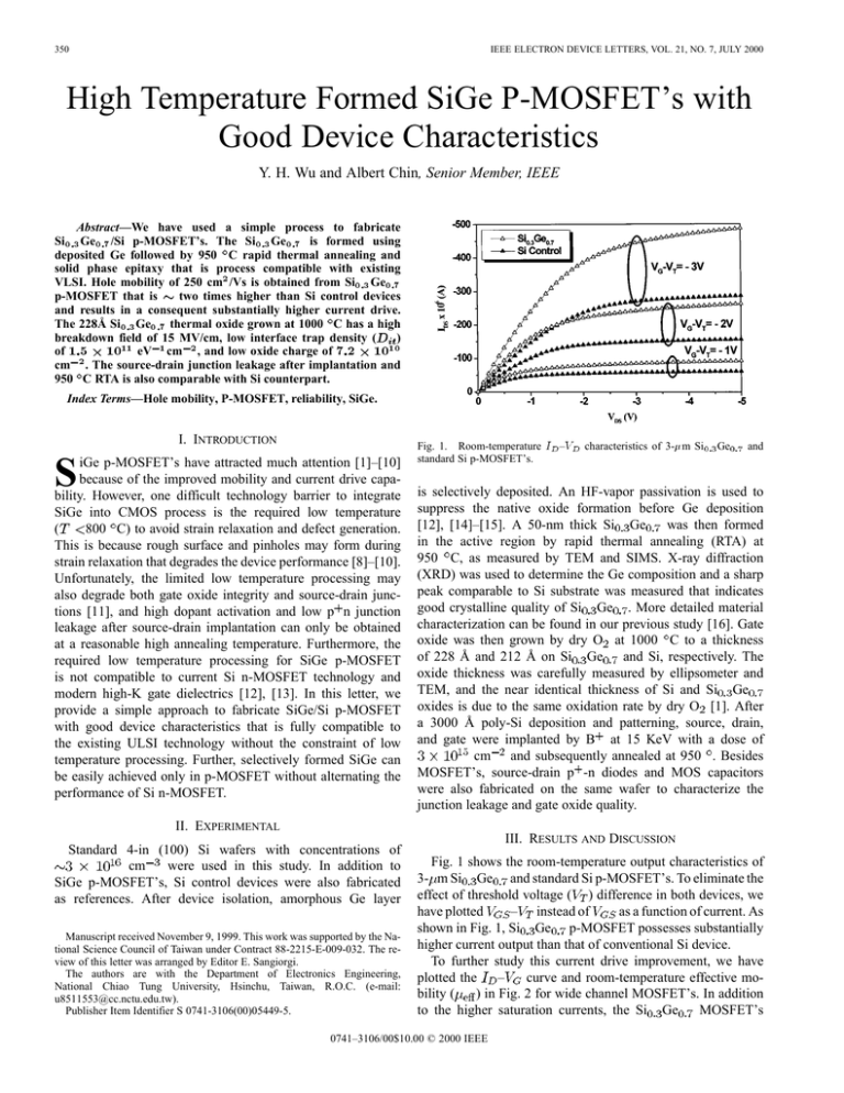
350 IEEE ELECTRON DEVICE LETTERS, VOL. 21, NO. 7, JULY 2000 High Temperature Formed SiGe P-MOSFET’s with Good Device Characteristics Y. H. Wu and Albert Chin, Senior Member, IEEE Abstract—We have used a simple process to fabricate Si0 3 Ge0 7 /Si p-MOSFET’s. The Si0 3 Ge0 7 is formed using deposited Ge followed by 950 C rapid thermal annealing and solid phase epitaxy that is process compatible with existing VLSI. Hole mobility of 250 cm2 /Vs is obtained from Si0 3 Ge0 7 p-MOSFET that is two times higher than Si control devices and results in a consequent substantially higher current drive. The 228Å Si0 3 Ge0 7 thermal oxide grown at 1000 C has a high breakdown field of 15 MV/cm, low interface trap density ( ) of 1 5 1011 eV 1 cm 2 , and low oxide charge of 7 2 1010 cm 2 . The source-drain junction leakage after implantation and 950 C RTA is also comparable with Si counterpart. Index Terms—Hole mobility, P-MOSFET, reliability, SiGe. I. INTRODUCTION S iGe p-MOSFET’s have attracted much attention [1]–[10] because of the improved mobility and current drive capability. However, one difficult technology barrier to integrate SiGe into CMOS process is the required low temperature 800 C) to avoid strain relaxation and defect generation. ( This is because rough surface and pinholes may form during strain relaxation that degrades the device performance [8]–[10]. Unfortunately, the limited low temperature processing may also degrade both gate oxide integrity and source-drain junctions [11], and high dopant activation and low p n junction leakage after source-drain implantation can only be obtained at a reasonable high annealing temperature. Furthermore, the required low temperature processing for SiGe p-MOSFET is not compatible to current Si n-MOSFET technology and modern high-K gate dielectrics [12], [13]. In this letter, we provide a simple approach to fabricate SiGe/Si p-MOSFET with good device characteristics that is fully compatible to the existing ULSI technology without the constraint of low temperature processing. Further, selectively formed SiGe can be easily achieved only in p-MOSFET without alternating the performance of Si n-MOSFET. Fig. 1. Room-temperature standard Si p-MOSFET’s. I –V characteristics of 3-m Si Ge and is selectively deposited. An HF-vapor passivation is used to suppress the native oxide formation before Ge deposition was then formed [12], [14]–[15]. A 50-nm thick Si Ge in the active region by rapid thermal annealing (RTA) at 950 C, as measured by TEM and SIMS. X-ray diffraction (XRD) was used to determine the Ge composition and a sharp peak comparable to Si substrate was measured that indicates good crystalline quality of Si Ge . More detailed material characterization can be found in our previous study [16]. Gate oxide was then grown by dry O at 1000 C to a thickness of 228 Å and 212 Å on Si Ge and Si, respectively. The oxide thickness was carefully measured by ellipsometer and TEM, and the near identical thickness of Si and Si Ge oxides is due to the same oxidation rate by dry O [1]. After a 3000 Å poly-Si deposition and patterning, source, drain, and gate were implanted by B at 15 KeV with a dose of cm and subsequently annealed at 950 . Besides MOSFET’s, source-drain p -n diodes and MOS capacitors were also fabricated on the same wafer to characterize the junction leakage and gate oxide quality. II. EXPERIMENTAL Standard 4-in (100) Si wafers with concentrations of cm were used in this study. In addition to SiGe p-MOSFET’s, Si control devices were also fabricated as references. After device isolation, amorphous Ge layer Manuscript received November 9, 1999. This work was supported by the National Science Council of Taiwan under Contract 88-2215-E-009-032. The review of this letter was arranged by Editor E. Sangiorgi. The authors are with the Department of Electronics Engineering, National Chiao Tung University, Hsinchu, Taiwan, R.O.C. (e-mail: u8511553@cc.nctu.edu.tw). Publisher Item Identifier S 0741-3106(00)05449-5. III. RESULTS AND DISCUSSION Fig. 1 shows the room-temperature output characteristics of 3- m Si Ge and standard Si p-MOSFET’s. To eliminate the effect of threshold voltage ( ) difference in both devices, we – instead of as a function of current. As have plotted shown in Fig. 1, Si Ge p-MOSFET possesses substantially higher current output than that of conventional Si device. To further study this current drive improvement, we have – curve and room-temperature effective moplotted the ) in Fig. 2 for wide channel MOSFET’s. In addition bility ( MOSFET’s to the higher saturation currents, the Si Ge 0741–3106/00$10.00 © 2000 IEEE WU AND CHIN: SiGe p-MOSFET’s WITH GOOD DEVICE CHARACTERISTICS Fig. 2. Room-temperature effective mobility for Si p-MOSFET’s derived from the insert I –V curves. Ge and Si 351 Fig. 4. Source-drain p n junction leakage distribution of Si measured at 3.3 V reverse bias. Ge and Si fect on mobility. The reason why this work enjoys much improved hole mobility could be attributed to extremely flat interface which is evidenced by TEM observation. Source-drain junction leakage is another important parameter for practical process integration. We have also measured the junction leakage and is shown in Fig. 4. Although the junction leakage of Si Ge is comparable with Si, the slightly higher value may be due to either lower bandgap or dislocation formation in Si Ge . This low junction leakage can be also explained by the high RTA annealing temperature for dopant activation and defect annihilation on high temperature formed Si Ge . Fig. 3. Gate oxide breakdown field distribution for thermal oxide grown on Si Ge and Si. The interface trap density is also shown in the inset figure. maintain the same subthreshold swing as Si counterpart. The Si Ge -channel devices has a peak hole mobility of 250 two times higher than Si control sample cm /Vs that is [17]. Because of the near identical measured capacitance for Si and Si Ge , the improved current drive capability is due MOSFET’s rather to the higher hole mobility in Si Ge than a higher-K [12]. In contrast to previous low temperature processed and strained p-MOSFET’s [1]–[9], the achieved good Si Ge mobility and device performance may be due to the high temperature formed and strain-relaxed Si Ge that results in a more stable material during thermal cycle [11],[18]–[19]. This is confirmed by the very sharp XRD linewidth after oxidation and post implantation RTA with near identical peak position and linewidth to as formed Si Ge . The higher mobility may be due to the smaller effective mass of Ge than Si even without strain [20]–[21]. We have also characterized the gate oxide integrity of high temperature formed Si Ge p-MOSFET’s. Fig. 3 shows the breakdown field distribution and the interface trap density of Si Ge gate oxide. The high breakdown electrical field of eV 15 MV/cm, low interface trap density ( ) of cm , and low oxide charge of cm indicate excellent oxide integrity can be achieved on high temperature formed in Si Ge may be due to Si Ge . The slightly higher Ge pile-up at oxide–SiGe interface, but it is still one order of magnitude lower than previous works [1] and has limited ef- IV. CONCLUSION We have demonstrated a simple method to fabricated SiGe p-MOSFET with good mobility, gate oxide integrity and junction leakage. Furthermore, this method is fully compatible to the existing VLSI technology. The good device performance is related to the high forming temperature of SiGe. ACKNOWLEDGMENT The authors would like to thank Prof. K. C. Hsieh, Department of Electrical Engineering, University of Illinois. REFERENCES [1] D. K. Nayak et al., “Wet oxidation of GeSi strained layers by rapid thermal processing,” Appl. Phys. Lett., vol. 57, pp. 369–371, 1990. [2] T. Manku and A. Nathan, “Lattice mobility of holes in strained and unstrained Si Ge alloys,” IEEE Electron Device Lett., vol. 12, pp. 704–706, Dec. 1991. [3] P. W. Li et al., “SiGe pMOSFET’s with gate oxide fabricated by microwave electron cyclotron resonance plasma processing,” IEEE Electron Device Lett., vol. 15, pp. 402–405, Oct. 1994. [4] S. P. Voinigescu, C. A. T. Salama, J. P. Noel, and T. I. Kamins, “Optimized Ge channel profiles for VLSI compatible Si/SiGe p-MOSFET’s,” in IEDM Tech. Dig., 1994, pp. 369–372. [5] M. A. Armstrong et al., “Design of Si/SiGe heterojunction complementary metal-oxide-semiconductor transistors,” in IEDM Tech. Dig., 1995, pp. 761–764. [6] G. Ternent et al., “SiGe p-channel MOSFET’s with tungsten gate,” Electron Lett., vol. 35, pp. 430–431, 1999. [7] H. Jiang and R. G. Elliman, “Electrical properties of GeSi surface- and buried-channel p-MOSFET’s fabricated by Ge implantation,” IEEE Trans. Electron Devices, vol. 43, pp. 97–103, Jan. 1996. [8] S. Verdonckt-Vandebroek et al., “SiGe-channel heterojunction p-MOSFET’s,” IEEE Trans. Electron Devices, vol. 41, pp. 90–101, Jan. 1994. 352 IEEE ELECTRON DEVICE LETTERS, VOL. 21, NO. 7, JULY 2000 [9] R. S. Prassad et al., “Mobility degradation in gated Si : SiGe quantum wells with thermally grown oxide,” Electron Lett., vol. 31, pp. 1876–1878, 1995. Ge channel metal-oxide-semi[10] K. Goto et al., “Fabrication of a Si conductor field-effect transistor (MOSFET) containing high Ge fraction layer by low-pressure chemical vapor deposition,” Jpn. J. Appl. Phys., vol. 32, pp. 438–441, 1993. [11] Y. Taur and T. K. Ning, Fundamental Modern VLSI Devices. Cambridge, U.K.: Cambridge Univ. Press, 1998, p. 286. [12] A. Chin, “Device and reiliability of high-k Al O gate dielecric with good mobility and low ,” in Proc. Symp. VLSI Tech., 1999, pp. 135–136. [13] S. C. Song et al., ““Ultrathin high quality stack nitride/oxide gate dielectrics prepared by in-situ rapid thermal N O oxidation of NH -nitride Si,” in Proc. Symp. VLSI Tech., 1999, pp. 137–138. [14] Y. H. Wu et al., “Improved electrical characteristics of CoSi using HF-vapor pretreatment,” IEEE Electron Device Lett., vol. 20, pp. 200–202, May 1999. [15] A. Chin et al., “The effect of native oxide on thin gate oxide integrity,” IEEE Electron Device Lett., vol. 19, pp. 426–428, Nov. 1998. D [16] Y. H. Wu, W. J. Chen, A. Chin, and C. Tsai, “The effect of native oxide on epitaxial SiGe from deposited amorphous Ge on Si,” Appl. Phys. Lett., vol. 74, pp. 528–530, 1999. [17] P. M. Garone, V. Venkataraman, and J. C. Sturn, “Hole mobility /Si heterostructure inversion enhancement in MOS-Gated Ge Si layers,” IEEE Electron Device Lett., vol. 13, pp. 56–58, Jan. 1992. [18] T. E. Jackman, J. M. Baribeau, and D. J. Lockwood, “Thermal stability of the [(Si) /(Ge) ] superlattice interface,” Phys. Rev. B, vol. 45, pp. 13 591–13 594, 1992. [19] P. Y. Wang et al., “Transition of carrier distribution from a strained to relaxed state in InGaAs/GaAs quantum well,” J. Appl. Phys., vol. 85, pp. 2985–2987, 1999. [20] T. Manku and A. Nathan, “Lattice mobility of holes in strained and unstrained SiGe alloys,” IEEE Electron Device Lett., vol. 12, pp. 704–706, Dec. 1991. [21] S. M. Sze, Physics of Semiconductor Devices. New York: Wiley, 1981, p. 850.


