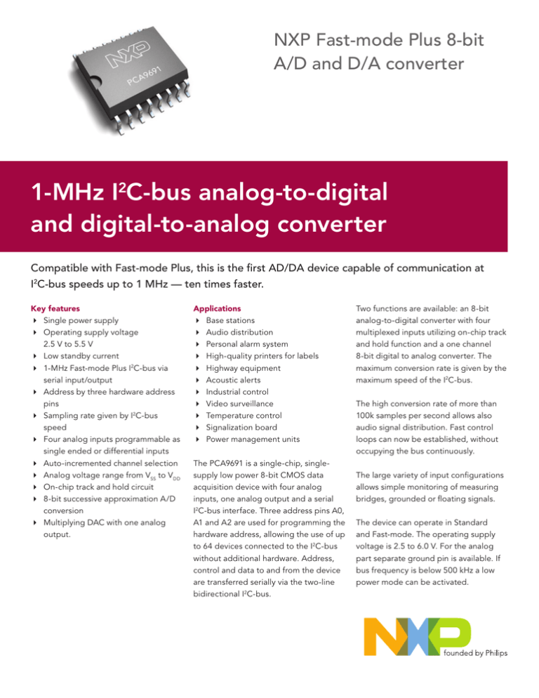
NXP Fast-mode Plus 8-bit
A/D and D/A converter
1-MHz I2C-bus analog-to-digital
and digital-to-analog converter
Compatible with Fast-mode Plus, this is the first AD/DA device capable of communication at
I2C-bus speeds up to 1 MHz — ten times faster.
Key features
4 Single power supply
4 Operating supply voltage 2.5 V to 5.5 V
4 Low standby current
4 1-MHz Fast-mode Plus I2C-bus via
serial input/output
4 Address by three hardware address
pins
4 Sampling rate given by I2C-bus
speed
4 Four analog inputs programmable as
single ended or differential inputs
4 Auto-incremented channel selection
4 Analog voltage range from VSS to VDD
4 On-chip track and hold circuit
4 8 -bit successive approximation A/D
conversion
4 Multiplying DAC with one analog
output.
Applications
4 Base stations
4 Audio distribution
4 Personal alarm system
4 High-quality printers for labels
4 Highway equipment
4 Acoustic alerts
4 Industrial control
4 Video surveillance
4 Temperature control
4 Signalization board
4 Power management units
The PCA9691 is a single-chip, singlesupply low power 8-bit CMOS data
acquisition device with four analog
inputs, one analog output and a serial
I2C-bus interface. Three address pins A0,
A1 and A2 are used for programming the
hardware address, allowing the use of up
to 64 devices connected to the I2C-bus
without additional hardware. Address,
control and data to and from the device
are transferred serially via the two-line
bidirectional I2C-bus.
Two functions are available: an 8-bit
analog-to-digital converter with four
multiplexed inputs utilizing on-chip track
and hold function and a one channel
8-bit digital to analog converter. The
maximum conversion rate is given by the
maximum speed of the I2C-bus.
The high conversion rate of more than
100k samples per second allows also
audio signal distribution. Fast control
loops can now be established, without
occupying the bus continuously.
The large variety of input configurations
allows simple monitoring of measuring
bridges, grounded or floating signals.
The device can operate in Standard
and Fast-mode. The operating supply
voltage is 2.5 to 6.0 V. For the analog
part separate ground pin is available. If
bus frequency is below 500 kHz a low
power mode can be activated.
The I2C-bus clock frequency is 0 to 1
MHz, and the SDA and SCL outputs are
capable of driving 30 mA. The operating
temperature range is –40 to +85 ºC.
SCL
SDA
A0
A1
I2C-bus
interface
Status
register
PCA9691
A2
ESD protection exceeds 2000V HBM per JESD22-A114, 200V MM per JESD22A115, and 1000V CDM per JESD22C101. Latch-up testing, performed
in accordance with JEDEC Standard
JESD78, exceeds 100 mA.
For more information visit www.nxp.com/i2clogic
DAC data
register
ADC data
register
EXT
VDD
VSS
Power on
reset
Control
logic
Oscillator
OSC
AIN0
AIN1
AIN2
Analog
multiplexer
–
Sample
and hold
AIN3
AOUT
Successive approximation
register/logic
+
Comparator
Sample
and hold
DAC
PCA9691 block diagram
Comparison of PCF8591 and PCA9691 A/D, D/A converter
Characteristics
PCA9691
PCF8591
1000 kHz
100 kHz
Voltage range
Maximum I2C-bus frequency
Maximum conversion rate
110,000 samples / sec
11,000 samples / sec
Number of device addresses
64
8
Ordering information
Package
Tube, 112
DIP 16
PCF8591P
SO 16
PCA9691T, PCF8591T
PCA9691T, PCF8591T
PCA9691BS
HVQFN 20
TSSOP16
Tape and Reel, 118
PCA9691TS
PCA9691TS
www.nxp.com
© 2006 NXP N.V.
All rights reserved. Reproduction in whole or in part is prohibited without the prior written consent of the copyright owner. The
Date of release: November 2006
information presented in this document does not form part of any quotation or contract, is believed to be accurate and reliable and
Document order number: 9397 750 15685
may be changed without notice. No liability will be accepted by the publisher for any consequence of its use. Publication thereof
Printed in the USA
does not convey nor imply any license under patent- or other industrial or intellectual property rights.
VREF
AGND


