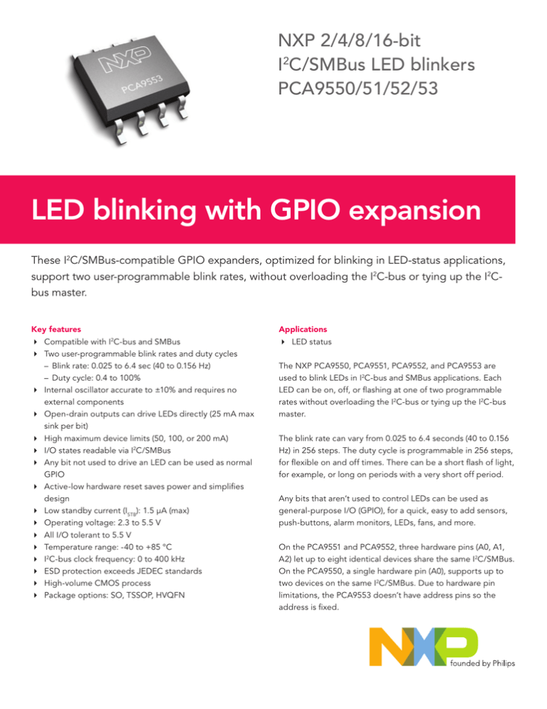
NXP 2/4/8/16-bit
I2C/SMBus LED blinkers
PCA9550/51/52/53
LED blinking with GPIO expansion
These I2C/SMBus-compatible GPIO expanders, optimized for blinking in LED-status applications,
support two user-programmable blink rates, without overloading the I2C-bus or tying up the I2Cbus master.
Key features
4 Compatible with I2C-bus and SMBus
4 Two user-programmable blink rates and duty cycles
– Blink rate: 0.025 to 6.4 sec (40 to 0.156 Hz)
– Duty cycle: 0.4 to 100%
4 Internal oscillator accurate to ±10% and requires no
external components
4 Open-drain outputs can drive LEDs directly (25 mA max
sink per bit)
4 High maximum device limits (50, 100, or 200 mA)
4 I/O states readable via I2C/SMBus
4 Any bit not used to drive an LED can be used as normal
GPIO
4 Active-low hardware reset saves power and simplifies
design
4 Low standby current (ISTB): 1.5 µA (max)
4 Operating voltage: 2.3 to 5.5 V
4 All I/O tolerant to 5.5 V
4 Temperature range: -40 to +85 °C
4 I2C-bus clock frequency: 0 to 400 kHz
4 ESD protection exceeds JEDEC standards
4 High-volume CMOS process
4 Package options: SO, TSSOP, HVQFN
Applications
4 LED status
The NXP PCA9550, PCA9551, PCA9552, and PCA9553 are
used to blink LEDs in I2C-bus and SMBus applications. Each
LED can be on, off, or flashing at one of two programmable
rates without overloading the I2C-bus or tying up the I2C-bus
master.
The blink rate can vary from 0.025 to 6.4 seconds (40 to 0.156
Hz) in 256 steps. The duty cycle is programmable in 256 steps,
for flexible on and off times. There can be a short flash of light,
for example, or long on periods with a very short off period.
Any bits that aren’t used to control LEDs can be used as
general-purpose I/O (GPIO), for a quick, easy to add sensors,
push-buttons, alarm monitors, LEDs, fans, and more.
On the PCA9551 and PCA9552, three hardware pins (A0, A1,
A2) let up to eight identical devices share the same I2C/SMBus.
On the PCA9550, a single hardware pin (A0), supports up to
two devices on the same I2C/SMBus. Due to hardware pin
limitations, the PCA9553 doesn’t have address pins so the
address is fixed.
2
LED1
3
VSS
4
16 VDD
A0
1
16 VDD
15 SDA
A1
2
15 SDA
14 SCL
A2
3
14 SCL
LED0
4
LED1
5
LED2
6
LED3
7
10 LED5
VSS
8
9
13 RESET
SLAVE ADDRESS
1
1
0
0
0
FIXED
0
A0
R/W
PROGRAMMABLE
13 RESET
12 LED7
11 LED6
LED4
SLAVE ADDRESS
PCA9550
1
Except for the number of bits and address pins, the functional
diagram and I/O schematic are the same for all of the devices.
A0
1
24 VCC
A1
2
23 SDA
1
0
3
22 SCL
4
21 RESET
LED1
5
20 LED15
LED2
6
LED3
7
LED4
8
LED5
9
16 LED11
LED0
1
LED6
10
15 LED10
LED1
2
LED7
11
14
LED9
LED2
3
VSS
12
13 LED8
VSS
4
0
FIXED
A2
A0
R/W
PROGRAMMABLE
19 LED14
18 LED13
17 LED12
16 VDD
15 SDA
14 SCL
13 LED3
SLAVE ADDRESS
SLAVE ADDRESS
0
A1
PCA9551
A2
1
A2
FIXED
LED0
1
0
PCA9553
ESD protection exceeds 2000 V HBM per JESD22-A114, 150
V MM per JESD22-A115, and 1000 V CDM per JESD22-C101.
JESDEC Standard JESD78 latch-up testing exceeds 100 mA.
More information on NXP LED blinkers can be found in
application note AN264.
PCA9551
1
PCA9552
On the PCA9550, PCA9551, and PCA9552, an external activelow reset hardware pin (RESET) returns registers to their
default states, without having to cycle power to the equipment,
if the I2C-bus locks up.
A0
LED0
PCA9550
Each device features open-drain outputs that sink 25 mA per
bit. The PCA9550 supports a maximum of 50 mA, the PCA9551
and PCA9553 a maximum of 100 mA, and the PCA9552 a
maximum of 200 mA (100 mA per 8-bit group).
A1
A0
1
R/W
1
0
0
0
1
0
R/W
FIXED
PROGRAMMABLE
PCA9553/01
PCA9552
Pin configuration
A2 A1 A0
3.3 V
INPUT
REGISTER
SCL
SDA
INPUT
FILTERS
PC BUS
CONTROL
LEDs
LED SELECT (LSx)
REGISTER
VCC
SDA
SDA
LED0
SCL
SCL
LED1
RESET
0
VDD
RESET
LED3
1
POWER ON
RESET
PRESCALER 0
REGISTER
PRESCALER 1
REGISTER
OSCILLATOR
LED2
LED4
LEDs
PWM0
REGISTER
BLINK0
PWM1
REGISTER
BLINK1
BUS MASTER
A0
LED5
A1
LED6
A2
GPIO
LED7
VSS
VSS
Note: only one I/D shown for clarity
Block diagram
PCA9551
Typical application
Order information
Package
Container
PCA9550
PCA9551
PCA9552
PCA9553/01
SO
Tube
T&R
PCA9550D
PCA9550D-T
PCA9551D
PCA9551D-T
PCA9552D
PCA9552D-T
PCA9553D/01
PCA9553D-T/01
TSSOP
Tube
T&R
PCA9550DP-T
PCA9551PW
PCA9551DP-T
PCA9552PW
PCA9552DP-T
PCA9553DP/01-T
HVQFN
T&R
PCA9551BS-T
PCA9552BS-T
www.nxp.com
© 2007 NXP N.V.
All rights reserved. Reproduction in whole or in part is prohibited without the prior written consent of the copyright owner. The
Date of release: June 2007
information presented in this document does not form part of any quotation or contract, is believed to be accurate and reliable and
Document order number: 9397 750 16021
may be changed without notice. No liability will be accepted by the publisher for any consequence of its use. Publication thereof
Printed in the USA
does not convey nor imply any license under patent or other industrial or intellectual property rights.


