UNIVERSITY OF OSLO Faculty of Mathematics and Natural Sciences
advertisement

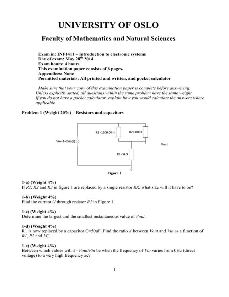
UNIVERSITY OF OSLO Faculty of Mathematics and Natural Sciences Exam in: INF1411 – Introduction to electronic systems Day of exam: May 28th 2014 Exam hours: 4 hours This examination paper consists of 6 pages. Appendices: None Permitted materials: All printed and written, and pocket calculator Make sure that your copy of this examination paper is complete before answering. Unless explicitly stated, all questions within the same problem have the same weight If you do not have a pocket calculator, explain how you would calculate the answers where applicable Problem 1 (Weight 20%) – Resistors and capacitors R2=10kΩ R3=15ΩkOhm Vin=1+2sin(t) Vout R1=5kΩ Figure 1 1-a) (Weight 4%) If R1, R2 and R3 in figure 1 are replaced by a single resistor RX, what size will it have to be? 1-b) (Weight 4%) Find the current i1 through resistor R1 in Figure 1. 1-c) (Weight 4%) Determine the largest and the smallest instantaneous value of Vout. 1-d) (Weight 4%) R1 is now replaced by a capacitor C=50uF. Find the ratio A between Vout and Vin as a function of R1, R2 and XC. 1-e) (Weight 4%) Between which values will A=Vout/Vin be when the frequency of Vin varies from 0Hz (direct voltage) to a very high frequency ac? 1 Problem 2 (Weight 17,5 %) – Diodes Figure 2: Diode characteristics 2-a) (Weight 5%) Given the diode characteristics of figure 2: Find approximate values for the diode resistance when VR =-60volt, VF = 0,5volt and VF = 0,8volt, respectively. 2-b) (Weight 5%) V=1 volt R V=sin(t) volt Figure 3: Diode circuit The circuit of figure 3 consists of an ac source, a battery, a diode and a resistor. Assume that the diode has ideal characteristics with a barrier voltage of 0,7volts. Furthermore assume that R=10kΩ. Find the value of the current through R when V=sin(t) has a) the most positive value and b) the most negative value. 2-c) (Weight 7,5%) Function of a diode circuit Figure 4 shows a digital circuit with two diodes and a bipolar transistor. Va, Vb and Vout are digital signals which either take the value of 0 volt or +5 volt, i.e. logic “0” or “1”. You can assume that the threshold voltage of the transistor is larger than the barrier voltage of the diode. Explain which Boolean function the circuit performs. (Hint: Identify which function the transistor has first). 2 +Vcc=5volt R2 R1 Vout Va Vb Figure 4: Digital logic circuit with transistor and diodes Problem (Weight 22,5 %) – Operational amplifiers 3-a) (Weight 5%) Opamp circuit V1 R1=4,7kΩ Rf=14,1kΩ R2=4,7kΩ + V2 V3 Vout R3=4,7kΩ Figure 5 3a-1) What is the circuit in Figure 5 called? 3a-2) Determine the amplification of the circuit 3a-3) Find V3 in the case of V1=1volt, V2=-2volt and Vout = -8volt 3-b) (Weight 7,5%) Active filtres Vout + Vin R C Figur 6: Active filter 3b-1) What is the difference between and active and a passive filter? 3b-2) If the input Vin is a dc voltage or an ac voltage with a low frequency, what function does the circuit in figure 6 perform (in addition to being a filter)? 3b-3) What is the value of A in the pass band of the filter in Figur 6, assuming all components are ideal? Justify briefly. 3 3-c) (Weight5%) Integrator C - Vin R Vout + Figure 7: Integrator The circuit in figure 7 is called an integrator. Draw the output signal Vout of the integrator when Vin is a square wave signal with a duty cycle of 50% and centered around 0 volt (i.e. a balanced signal) 3-d) (Weight 5%) What happens to the output signal in problem 3-c) if the opamp no longer is ideal, but suffers from a constant offset such that Vout >0V when Vin=0V? Justify your answer! Problem 4 (Weight 20 %) – Transistors 4-a) (Weight 5%) Given the transistor in figure 8: Internally in the transistor there is a fault either in the base, the collector or the emitter, and measurements on the terminals reveal that VB=3 volt and VC=9 volt (see the drawing). Assume a threshold voltage of VTH= 0.7 volt. Is the internal fault either in the base, the collector or in the emitter? Justify your answer! Vcc +9 v RC=560 Ohm 9v 3v VBB=3v RB=56 kOhm Figure 8: BJT with an internal fault 4-b) (Weight 2,5%) Vcc=25volt R1=44kΩ RC=2kΩ R2=10kΩ RE=2kΩ Figure 9 4 What are the functions of the resistors RE and RC in Figure 9? What will happen if both resistors are removed and the emitter is connected directly to ground and the collector directly to Vcc? 4c) (Weight 2,5%) If IE=4mA and IB=10µA, what will be the values of IC and β? 4e) (Weight 5%) Assume now that the resistor R2 in Figure 9 has an unknown value. What is the smallest value R2 must have in order to prevent the transistor from being in cutoff? Assume VTH=0.7 volt 4d) (Weight 5%) Vcc R1 Vcc RC R1 Vout1 Vin2 Vin1 Vout2 R2 R2 RE RE Figure 10: BJT amplifier circuits What is the phase shift between Vin1 and Vout1, and between Vin2 and Vout2 in the amplifier circuits in Figure 10? Explain and justify your answer! Problem 5 (Weight 20 %) – Multiple choice 5-a) Current, voltage and impedance Which statement is correct? 1) The sum of the voltages around a closed loop equals the sum of the impedances around the same loop 2) The sum of the impedances around a closed loop is independent of frequency 3) The sum of the currents entering a node has the same sign as the voltage of that node with respect to ground 4) Whether the voltages are algebraically added clockwise or counter-clockwise does not matter when applying KVL 5) KVL does not apply to circuits containing reactive elements 5-b) Capacitors Which statement is correct? 1) A capacitor stores electrical current 2) A capacitor stores electrcal charge 3) The impedance of a capacitor is independent of frequency 4) Another name for the impedance of a capacitor is inductive reactance 5) The inverse of capacitive reactance is reactive impedance 5 5-c) DA converters Which statement is correct? 1) The resolution of a DA converter can’t improve the resolution of the input signal 2) DA converters always require a clock signal to function 3) DA converters use an internal AD converter as a voltage reference 4) Digital signals can have infinite resolution as opposed to analog signals 5) Operational amplifiers cannot be used in DA converters 5-d) AD converters Which statement is correct? 1) An AD converter converts an analog current to a digital voltage 2) If a DA converter is connected to the output of an AD converter, the resolution of the analog signal is not altered end-to-end 3) AD converters cannot be used in net pads 4) AD converters can convert both currents and voltages 5) High-frequency non-periodic noise in the analog signal being converted will always propagate to the digital signal 5-e) Transistors Which statement is correct? 1) Bipolar transistors are independent current sources 2) Bipolar transistors are independent voltage sources 3) Bipolar transistors are current controlled current sources 4) Bipolar transistors are voltage controlled voltage sources 5) All bipolar transistors have the same current amplification 6


