CDB5333
Evaluation Board for CS5333
Features
Description
l Demonstrates
The CDB5333 evaluation board is an excellent means
for quickly evaluating the CS5333 24-bit, stereo A/D converter. Evaluation requires a digital signal analyzer, an
analog signal source, and a power supply.
recommended layout and
grounding arrangements
l CS8404A generates AES/EBU, S/PDIF, and
EIAJ-340 compatible digital audio
l Requires only an analog signal source and
power supplies for a complete Analog-toDigital-Converter system
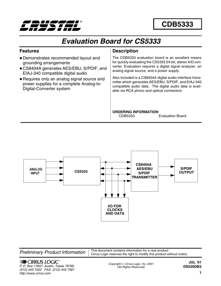
Also included is a CS8404A digital audio interface transmitter which generates AES/EBU, S/PDIF, and EIAJ-340
compatible audio data. The digital audio data is available via RCA phono and optical connectors.
ORDERING INFORMATION
CDB5333
Evaluation Board
$1$/2*
,1387
CS8404A
AES/EBU
S/PDIF
TRANSMITTER
CS5333
S/PDIF
OUTPUT
I/O FOR
CLOCKS
AND DATA
Preliminary Product Information
P.O. Box 17847, Austin, Texas 78760
(512) 445 7222 FAX: (512) 445 7581
http://www.cirrus.com
This document contains information for a new product.
Cirrus Logic reserves the right to modify this product without notice.
Copyright Cirrus Logic, Inc. 2001
(All Rights Reserved)
JUL ‘01
DS520DB3
1
CDB5333
TABLE OF CONTENTS
1.
2.
3.
4.
5.
6.
CDB5333 SYSTEM OVERVIEW .............................................................................................. 3
CS5333 ANALOG TO DIGITAL CONVERTER ........................................................................ 3
CS8404A DIGITAL AUDIO TRANSMITTER ............................................................................ 3
INPUT/OUTPUT FOR CLOCKS AND DATA ........................................................................... 3
POWER SUPPLY CIRCUITRY ................................................................................................. 3
GROUNDING AND POWER SUPPLY DECOUPLING ............................................................ 3
LIST OF FIGURES
Figure 1. System Block Diagram and Signal Flow .......................................................................... 5
Figure 2. Analog Audio Input........................................................................................................... 6
Figure 3. CS5333 ............................................................................................................................ 7
Figure 4. Reset Circuit..................................................................................................................... 7
Figure 5. Level Shifters ................................................................................................................... 8
Figure 6. I/O for Clocks/Data........................................................................................................... 9
Figure 7. CS8404A Digital Audio Interface...................................................................................... 9
Figure 8. Digital Audio Output ....................................................................................................... 10
Figure 9. Power Circuit.................................................................................................................. 11
Figure 10. Top Layer Silkscreen ................................................................................................... 12
Figure 11. Top Layer ..................................................................................................................... 13
Figure 12. Bottom Layer................................................................................................................ 14
LIST OF TABLES
Table 1. System Connections ........................................................................................................ 4
Table 2. CDB5333 Jumper and Switch Settings ............................................................................ 4
Contacting Cirrus Logic Support
For a complete listing of Direct Sales, Distributor, and Sales Representative contacts, visit the Cirrus Logic web site at:
http://www.cirrus.com/corporate/contacts/
Preliminary product information describes products which are in production, but for which full characterization data is not yet available. Advance product information describes products which are in development and subject to development changes. Cirrus Logic, Inc. has made best efforts to ensure that the information
contained in this document is accurate and reliable. However, the information is subject to change without notice and is provided “AS IS” without warranty of
any kind (express or implied). Customers are advised to obtain the latest version of relevant information to verify, before placing orders, that information being
relied on is current and complete. All products are sold subject to the terms and conditions of sale supplied at the time of order acknowledgment, including those
pertaining to warranty, patent infringement, and limitation of liability. No responsibility is assumed by Cirrus Logic, Inc. for the use of this information, including
use of this information as the basis for manufacture or sale of any items, nor for infringements of patents or other rights of third parties. This document is the
property of Cirrus Logic, Inc. and by furnishing this information, Cirrus Logic, Inc. grants no license, express or implied under any patents, mask work rights,
copyrights, trademarks, trade secrets or other intellectual property rights of Cirrus Logic, Inc. Cirrus Logic, Inc., copyright owner of the information contained
herein, gives consent for copies to be made of the information only for use within your organization with respect to Cirrus Logic integrated circuits or other parts
of Cirrus Logic, Inc. The same consent is given for similar information contained on any Cirrus Logic website or disk. This consent does not extend to other
copying such as copying for general distribution, advertising or promotional purposes, or for creating any work for resale. The names of products of Cirrus Logic,
Inc. or other vendors and suppliers appearing in this document may be trademarks or service marks of their respective owners which may be registered in some
jurisdictions. A list of Cirrus Logic, Inc. trademarks and service marks can be found at http://www.cirrus.com.
2
DS520DB3
CDB5333
1. CDB5333 SYSTEM OVERVIEW
The CDB5333 evaluation board is an excellent
means of quickly evaluating the CS5333. The
CS8404A digital audio interface transmitter provides an easy interface to digital audio signal analyzers including the majority of digital audio test
equipment.
The CDB5333 schematic has been partitioned into
8 schematics shown in Figures 2 through 9. Each
partitioned schematic is represented in the system
diagram shown in Figure 1. Notice that the system
diagram also includes the interconnections between the partitioned schematics.
2. CS5333 ANALOG TO DIGITAL
CONVERTER
A description of the CS5333 is included in the
CS5333 datasheet.
3. CS8404A DIGITAL AUDIO
TRANSMITTER
The system generates and encodes standard
S/PDIF data using a CS8404A Digital Audio
Transmitter, Figure 7. The outputs of the CS8404A
are RS422 compatible differential line drivers. The
CS8404A data format has been configured for I2S.
A description of the CS8404A is included in the
CS8404A datasheet.
Note:
The CS8404A can not be the clock source for
the board
er, J6. The schematic for the clock/data input/output is shown in Figure 6.
The CDB5333 allows some flexibility as to the
generation of the clocks. When in slave mode, the
MCLK, SCLK, and LRCK must be provided via
the header, J6. When operating the CS5333 in master mode, MCLK is generated from the on board
oscillator, Y1. This oscillator is socketed to allow
other frequency oscillators to be used.
Note:
When providing MCLK externally, the on board
oscillator must be removed.
5. POWER SUPPLY CIRCUITRY
Power is supplied to the evaluation board by four
binding posts (GND, +5 V, VA, VL), see Figure 9.
The +5 V input supplies power to the +5 V digital
circuitry (+5 V) and the amplifiers (VAA_+5 V),
while the two +1.8/+3.3 V inputs supply power to
the VA and VL pins of the CS5333 and to the level
shifter circuits.
6. GROUNDING AND POWER SUPPLY
DECOUPLING
The CS5333 requires careful attention to power
supply and grounding arrangements to optimize
performance. Figure 3 details the power distribution used on this board. The decoupling capacitors
are located as close to the CS5333 as possible. Extensive use of ground plane fill in the evaluation
board yields large reductions in radiated noise.
4. INPUT/OUTPUT FOR CLOCKS AND
DATA
The evaluation board has been designed to allow
interfacing to external systems via the 10-pin head-
DS520DB3
3
CDB5333
CONNECTOR
INPUT/OUTPUT
SIGNAL PRESENT
+5 V
Input
+ 5 Volt power
VA
Input
+ 1.8 to + 3.3 Volt power for the CS5333
VL
Input
+ 1.8 to +3.3 Volt power for the CS5333
GND
Input
Ground connection from power supply
Left Audio In
Input
Analog input left channel
Right Audio In
Input
Analog input right channel
Optical Output
Output
Digital audio output
Coax Output
Output
Digital audio output
Table 1. System Connections
JUMPER /
SWITCH
PURPOSE
POSITION
FUNCTION SELECTED
J3
MCLK divide/Mode select HI
*LOW
Master: High Rate mode Slave: MCLK divide
Master: Base Rate mode Slave: NA
J4
Data format select
HI
*LOW
Left Justified, up to 24-bit data
I2S, up to 24-bit data
J5
MCLK divider for the
CS8404A
DIV1
*DIV2
DIV4
MCLK goes straight to CS8404A
MCLK divided by two prior to CS8404A
MCLK divided by four prior to CS8404A
J7
Master/Slave select for
CS5333
*HI
LOW
CS5333 in Master mode
CS5333 in Slave mode
J6
Input/Output for
clocks/data
-
-
S1
Reset for the CDB5333
-
-
Notes:
* denotes default factory settings
Table 2. CDB5333 Jumper and Switch Settings
4
DS520DB3
DS520DB3
FIG 2
INPUTS
ANALOG
FIG 5
SHIFTER
LEVEL
I/O FOR
FIG 6
AND DATA
CLOCKS
Figure 1. System Block Diagram and Signal Flow
FIG 3
CS5333
FIG 4
CIRCUIT
RESET
FIG 7
INTERFACE
AUDIO
DIGITAL
CS8404A
FIG 8
OUTPUTS
DIGITAL
CDB5333
5
Figure 2. Analog Audio Input
CDB5333
6
DS520DB3
CDB5333
Figure 3. CS5333
Figure 4. Reset Circuit
DS520DB3
7
CDB5333
Figure 5. Level Shifters
8
DS520DB3
CDB5333
Figure 6. I/O for Clocks/Data
Figure 7. CS8404A Digital Audio Interface
DS520DB3
9
CDB5333
Figure 8. Digital Audio Output
10
DS520DB3
CDB5333
Figure 9. Power Circuit
DS520DB3
11
Figure 10. Top Layer Silkscreen
CDB5333
12
DS520DB3
Figure 11. Top Layer
CDB5333
DS520DB3
13
Figure 12. Bottom Layer
CDB5333
14
DS520DB3
• Notes •


