High frequency schnuffler/sniffer kit(version 2)
advertisement

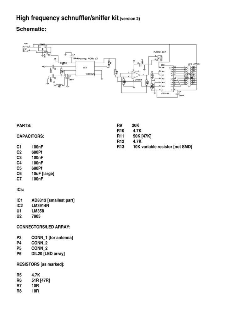
High frequency schnuffler/sniffer kit (version 2) Schematic: PARTS: CAPACITORS: C1 C2 C3 C4 C5 C6 C7 100nF 680Pf 100nF 100nF 680Pf 10uF [large] 100nF ICs: IC1 IC2 U1 U2 AD8313 [smallest part] LM3914N LM358 7805 CONNECTORS/LED ARRAY: P3 P4 P5 P6 CONN_1 [for antenna] CONN_2 CONN_2 DIL20 [LED array] RESISTORS [as marked]: R5 R6 R7 R8 4.7K 51R [47R] 10R 10R R9 R10 R11 R12 R13 20K 4.7K 50K [47K] 4.7K 10K variable resistor [not SMD] Images: Description: The circuit detects, demodulates the amplitude and amplifies high frequency electromagnetic emissions (100 MHz to 2.5 GHz approx) for audio frequency output and level display. The main component is the Analog Devices AD8313 IC: RF logarithmic detector and controller, whose output is further amplified by the LM358 op-amp for a mic input level signal. This signal provides an input for the LM3914 display driver IC which controls the LED bar. Construction notes: Clean the board first with pure alcohol. All parts will be soldered from above with the copper facing you. Solder the AD8313 chip first, taking care of orientation. With the board facing you and xxxxx text in the bottom left corner as in the photograph above, the arrow (within darker square) should be in the top right corner and the dot top left. Soldering technique for small parts: Place first a very small blob of solder on the top left two pins and place the chip carefully here, reheating the solder to place the IC in the right position. Carefully solder the remaining pins in place. use the golden solder braid to mop up any solder bridges, putting the braid next to the bridge and heating the braid with the soldering iron to soak up excess solder. Check that the AD8313 is properly soldered using a magnifying glass. Next solder the remaining surface mount components, starting with the LM358 which should be placed with the bar on the left, all resistors and capacitors. Trim the legs of the LM3914 chip and solder this in place with pin one in the top left. Solder the LED array carefully, as there is not much room to fit the soldering iron underneath. Make sure that the array is placed with the text on the right hand side. Next, trim the legs of the 7805 voltage regulator and solder in place with the metal surface facing away, solder the larger 10uF electrolytic capacitor with - (white bar) to the left, solder a small jumper for audio to P5 marked. Solder the small potentiometer with one outside pin on the right side of R13 and the other two pins to the large copper ground surface. Solder a small wire bridge between the two open points as pictured in green. Attach the red and black wires of the 9v connector in the top left of the board with black going to the large ground plane and red to the + input of the voltage regulator. Attach a short antenna wire to P3. The device is now ready for testing - the variable resistor/potentiometer is adjusted for offset. References: http://f6bon.albert.free.fr/Milliwattmetre.html http://www.analog.com/en/prod/0%2c%2c770_847_AD8313%2c00.html http://www.turnpoint.net/wireless/cantennahowto.html http://www.engadget.com/2005/11/15/how-to-build-a-wifi-biquad-dish-antenna/ http://1010.co.uk m@1010.co.uk


