Freescale Semiconductor
Advance Information
Document Number: MC33288
Rev 6.0, 5/2006
Solid State Relay for
Automotive Flasher
Applications
33288
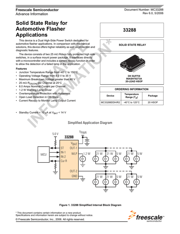
This device is a Dual High-Side Power Switch dedicated for
automotive flasher applications. In comparison with mechanical
solutions, this device offers higher reliability as well as protection and
diagnostic features.
The device consists of two 25 mΩ Rdson fully protected high side
switches, in a surface mount power package. It interfaces directly
with a microcontroller and includes a current recopy function in order
to allow the detection of a failed lamp in the application.
Features
• Junction Temperature Range from -40°C to 150°C
• Operating Voltage Range from 8.0 V to 35 V
• Maximum Breakdown Voltage greater than 40 V
• 25 mΩ RDS(ON) per Channel at 25°C
• 8.0 Amps Nominal Current per Channel
• 1.2 W Warning Lamp Driver
• Overtemperature Protection with Hysteresis
• Open Load Detection in ON State
• Current Recopy to Monitor Lamp Output Current
SOLID STATE RELAY
DH SUFFIX
98ASH70273A
20-LEAD HSOP
ORDERING INFORMATION
Device
Temperature
Range (TA)
Package
MC33288DDH/R2
-40°C to 125°C
20 HSOP
• Standby Current < 10 µA at VBAT < 14 V
Simplified Application Diagram
5.0 V
VPWR
33288
VBAT
MCU
ST
OUT-1
IN-1
WLP
IN-2
Cur R
1.2 W
21 W
21 W
5W
21 W
5W
21 W
21 W
5W
21 W
5W
OUT-2
GND
Figure 1. 33288 Simplified Internal Block Diagram
* This document contains certain information on a new product.
Specifications and information herein are subject to change without notice.
© Freescale Semiconductor, Inc., 2006. All rights reserved.
TERMINAL CONNECTIONS
TERMINAL CONNECTIONS
VBAT
21
GND
CUR R
IN1
NC
DNC
OUT1
OUT1
OUT1
NC
NC
1
2
3
4
5
6
7
8
9
10
20
19
18
17
16
15
14
13
12
11
WLP
STATUS
IN2
NC
DNC
OUT2
OUT2
OUT2
NC
NC
21
VBAT
Figure 2. 33288 Terminal Connections
Table 1. 33288 Terminal Definitions
A functional description of each terminal can be found in the Functional Description section beginning on 7.
Terminal
Number
Terminal
Name
Formal Name
TAB
VBAT
Supply Voltage
2
CUR R
Load Current Sense
3
IN1
INPUT Channel 1
18
IN2
INPUT Channel 2
4, 9, 10, 11,
12, 17
NC
No Connect
5, 16
DNC
Do Not Connect
6, 7, 8
OUT1
OUTPUT Channel 1
They deliver current to the connected loads and are controlled via the IN1 terminals.
13, 14, 15
OUT2
OUTPUT Channel 2
They deliver current to the connected loads and are controlled via the IN2 terminals,
11
GND
Ground
19
STATUS
Status for Both
Channels
20
WLP
Definition
The backside TAB is connected to the power supply of the MC33288DH.
The Current Sense terminal delivers a ratioed amount (1/1000) of the sum of the currents
that can be used to generate signal ground referenced output voltages for use by the
microcontroller.
These are the device input terminals which directly control their associated outputs.
These terminals are not used.
These terminals must not be connected.
This is the ground terminal of the device.
The Fault output is an open drain indication that goes active low when a fault mode
(Openload, Overtemperature) is detected by the device.
Warning Lamp Output It delivers current through the connected load.
33288
2
Analog Integrated Circuit Device Data
Freescale Semiconductor
MAXIMUM RATINGS
MAXIMUM RATINGS
Table 2. Maximum Ratings
All voltages are with respect to ground unless otherwise noted. Exceeding these ratings may cause a malfuncion or
permanent damage to the device.
Ratings
Symbol
Value
Unit
VBAT Voltage with Respect to GND : Continuous/Pulse
VBAT
-14 to 40
V
OUT1 and OUT2 Voltage with Respect to GND : Continuous/Pulse
VOUT
-0.3 to 40
V
OUT1 to VBAT and OUT2 to VBAT Voltage : Continuous/Pulse
VOUT
40
V
IN1, IN2, St DC Voltage : Continuous/Pulse
VIN
-0.3 to 7.0
V
CUR R Voltage : Continuous/Pulse
VCR
-0.3 to 7.0
V
Human Body Model (1)
VESD1
±2000
Machine Model (2)
VESD2
±200
IOUTP
40
A
IIN
±5.0
mA
TJ
-40 to 150
°C
TSTORAGE
-65 to 150
°C
RθJC
2.0
°C/W
RθJA
25
°C/W
PD
5.0
W
ELECTRICAL RATINGS
ESD All Pins
V
OUT1, OUT2 Output Current : Pulse (3)
IN1, IN2, STATUS
THERMAL RATINGS
Junction Temperature
Storage Temperature Range
Thermal Resistance Junction to Case
Thermal Resistance Junction to Ambient
(4)
Power Dissipation at Tcase 140°C (5)
Notes
1. ESD1 testing is performed in accordance with the Human Body Model (CZAP = 100 pF, RZAP = 1500 Ω).
2.
ESD2 testing is performed in accordance with the Machine Model (CZAP = 200 pF, RZAP = 0 Ω).
3.
During lamp inrush current.
4.
Device mounted on dual side printed circuit board with 70 µm copper thickness and 10 cm2 copper heat sink (2.5 cm2 on top side and
5.
7.5 cm2 on down side).
Assuming a 150°C maximum junction temperature.
33288
Analog Integrated Circuit Device Data
Freescale Semiconductor
3
STATIC ELECTRICAL CHARACTERISTICS
STATIC ELECTRICAL CHARACTERISTICS
Table 3. Static Electrical Charactersitics
Characteristics noted under conditions 4.5 V ≤ VDD ≤ 5.5 V, 9.0 V ≤ VPWR ≤ 16 V, -40°C ≤ TA ≤ 125°C, unless otherwise noted.
Typical values noted reflect the approximate parameter mean at TA = 25°C under nominal conditions, unless otherwise noted.
Characteristic
Symbol
Min
Typ
Max
Unit
Nominal Operating Voltage
VBAT
9
–
16
V
Functional Operating Voltage
VBAT
8
–
35
V
Under Voltage Threshold
VµV
6
7
8
V
–
1
10
–
8
20
–
20
25
–
30
40
POWER INPUT
VBAT Standby Supply Current
Supply Current in ON State
ION
IN1 and IN2 @ 3.5 V, no fault, VBAT < 14 V, TJ < 125°C
Drain to Source on Resistance
VBAT to Output Breakdown Voltage
IOL
–
A
–
4
–
–
1
–
40
–
–
–
–
10
–
–
10
VDSS
µA
µA
IOUT-LEAK
VIN2 = 0 V, VBAT = 35 V, VOUT2 = 0 V
A
A
IOUT-LEAK
VIN1 = 0 V, VBAT = 35 V, VOUT1 = 0 V
VBAT to OUT2 : Leakage Current
30
ILIM
IN1 and IN2 @ 0 V, VOUT = 0 V, IOUT -0.25 mA
VBAT to OUT1 : Leakage Current
A
–
VOUT < 1.0 V, TJ = 25°C
Hot Openload Threshold
mΩ
ILIM
VOUT > 1.0 V
Short Circuit limitation
mΩ
RDSON
IOUT = 4.0 A, VBAT > 9.0 V and TJ = 150°C
High Current Limitation
mA
RDSON
IOUT = 4.0 A, VBAT > 9.0 V and TJ = 25°C
Drain to Source on Resistance
µA
ISTDBY
VBAT < 14 V and VIN = 0 V, TJ < 125°C
VIN1, VIN2 : Input Voltage Low Threshold
VIL
–
–
1.5
V
VIN1, VIN2 : Input Voltage High Threshold
VIH
3.5
–
–
V
VIN1, VIN2 : Input Voltage Hysteresis
VIH
0.4
0.7
0.9
V
VIN1, VIN2 : Input Current
IIN
–
18
40
–
–
0.5
VIN1, VIN2 = 3.5 V
Status Output Voltage
µA
Vst
Ist = 1 mA; Output in Fault
V
Thermal Shutdown
TSHUT
150
–
–
°C
Thermal Shutdown Hysteresis
THYST
–
10
–
°C
33288
4
Analog Integrated Circuit Device Data
Freescale Semiconductor
STATIC ELECTRICAL CHARACTERISTICS
Table 3. Static Electrical Charactersitics(continued)
Characteristics noted under conditions 4.5 V ≤ VDD ≤ 5.5 V, 9.0 V ≤ VPWR ≤ 16 V, -40°C ≤ TA ≤ 125°C, unless otherwise noted.
Typical values noted reflect the approximate parameter mean at TA = 25°C under nominal conditions, unless otherwise noted.
Characteristic
Min
Typ
Max
–
1/1000
–
-10
–
10
–
1/1000
–
-20
–
20
VCLST
5.5
–
7.0
V
Nominal Flasher Frequency Operation
FFL
–
1.5
–
Hz
Frequency Operation
FOP
–
–
100
Hz
Nominal Flasher Duty Cycle Operation
DCFL
–
50
–
%
WLP Output Drain to Source on Resistance
RWON
Current Recopy Ratio
Symbol
µA
CR
VOUT > VBAT -1.0 V, IOUT from 2.0 A to 4.0 A
Unit
TJ -40°C to 105°C, VBAT 9.0 V to 16 V
Current Recopy Ratio Accuracy
CR-AC
VOUT > VBAT -1.0 V, IOUT from 2.0 A to 4.0 A
%
TJ -40°C to 105°C, VBAT 9.0 V to 16 V
Extended Current Recopy Ratio
CREX
VOUT > VBAT -1.0 V, IOUT from 1.0 A to 8.0 A
Extended Current Recopy Ratio Accuracy
CREX-AC
VOUT > VBAT -1.0 V, IOUT from 1.0 A to 8.0 A
Current Recopy Clamp Voltage At 10mA
IOUT = 100 mA, VBAT > 9.0 V and TJ = 25°C
WLP Output Drain to Source on Resistance
Ω
–
3.2
Ω
RWON
–
–
5.0
IWLIM
VOUT = 0 V
WLP Thermal Shutdown
%
–
IOUT = 100 mA, VBAT > 9.0 V and TJ = 125°C
WLP Output Current Limitation
%
TWSHUT
mA
–
500
–
150
–
–
°C
33288
Analog Integrated Circuit Device Data
Freescale Semiconductor
5
DYNAMIC ELECTRICAL CHARACTERISTICS
DYNAMIC ELECTRICAL CHARACTERISTICS
Table 4. Dynamic Electrical Characteristics
Characteristics noted under conditions 4.5 V ≤ VDD ≤ 5.5 V, 9.0 V ≤ VPWR ≤ 16 V, -40°C ≤ TA ≤ 125°C, unless otherwise noted.
Typical values noted reflect the approximate parameter mean at TA = 25°C under nominal conditions, unless otherwise noted.
Characteristic
Symbol
Min
Typ
Max
Unit
MICROCONTROLLER INTERFACE
Maximum Output Positive Slew Rate
tR
Load = 6.0 Ω
Maximum Output Negative Slew Rate
Load = 6.0 Ω, from VIN/2 to 90% VOUT
0.3
2.0
0.01
0.3
2.0
1.0
30
200
1.0
40
200
V/µs
µs
TDON
Load = 6.0 Ω, from VIN/2 to 10% VOUT
Turn OFF Delay Time
0.01
tF
Load = 6.0 Ω
Turn ON Delay Time
V/µs
µs
TDOFF
33288
6
Analog Integrated Circuit Device Data
Freescale Semiconductor
FUNCTIONAL DESCRIPTION
INTRODUCTION
FUNCTIONAL DESCRIPTION
INTRODUCTION
The MC33288DH is a dual high side switch with
appropriate control, protection, and diagnostic features
dedicated to automotive flasher applications. The device
consists of two independent 25mW power switches and an
additionnal 3.2 Ω high-side switch capable of controlling a 1.2
W warning lamp. It interfaces directly with a microcontroller
and the package used is a 20-HSOP power small outline, 20
terminals. The MC33288 incorporates a status terminal and
a load current sense capability.
FUNCTIONAL TERMINAL DESCRIPTIONS
SUPPLY VOLTAGE (VBAT)
The backside TAB is connected to the power supply of the
MC33288DH. In addition to its supply function, this terminal
contributes to the thermal behaviour of the device by
conducting the heat from the switching MOSFET to the
printed circuit board.
OUTPUT CHANNEL (OUT1, OUT2)
Pins 6, 7, and 8 are the source of the output 1 25 mΩ
MOSFET1. Pins 13, 14, and 15 are the source of the output
2 25 mΩ MOSFET2. They deliver current to the connected
loads and are controlled via the IN1 and IN2 terminals,
respectively . These outputs are current limited and
thermally protected.
LOAD CURRENT SENSE (CUR R)
The Current Sense terminal delivers a ratioed amount (1/
1000) of the sum of the currents that can be used to generate
signal ground referenced output voltages for use by the
microcontroller.
INPUT CHANNEL 1/2 (IN1, IN2)
These are the device input terminals which directly control
their associated outputs. The levels are CMOS compatible.
When the input is a logic low, the associated output MOSFET
is in the OFF state. When input is high, the MOSFET is turned
ON and the load is activated. When both inputs are low, the
device is in standby mode and its supply current is reduced.
Each input terminal has an internal active pull-down, so that
it will not float if disconnected.
GROUND (GND)
This is the ground terminal of the device.
STATUS FOR BOTH CHANNELS (STATUS)
The Fault output is an open drain indication that goes active
low when a fault mode (Openload, Overtemperature) is
detected by the device on either one channel or both
channels simultaneously. Its internal structure is an open
drain architecture with an internal clamp at 6.0 V. An
external pull-up resistor connected to VDD (5.0 V) is needed.
WARNING LAMP OUTPUT (WLP)
This terminal is the source of a 3.2 Ω MOSFET. This output
is current limited and thermally protected. It delivers current
through the connected load when both IN1 and IN2 inputs
are logic high. It is usually used as a warning lamp driver for
Flasher application.
33288
Analog Integrated Circuit Device Data
Freescale Semiconductor
7
FUNCTIONAL DEVICE OPERATION
OPERATIONAL MODES
FUNCTIONAL DEVICE OPERATION
OPERATIONAL MODES
Power Supply
The MC33288 can be directly connected to the supply line.
In standby mode (IN1 and IN2 @ OV), the supply current is
less than 10 mA for VBAT supply voltage below 14 V. This
feature allows a very low supply current on the battery when
the car is idle or parked.
During the OFF state, the current recopy terminal and the
status terminals are in high impedance.
In case of loss of (digital) ground, the power MOSFETs
turn off in order to safely tie the load current to zero.
Nominal Voltage and Transient Operation
The nominal operation voltage is from 9.0 V to 16 V. The
MC33288 is functional over a larger voltage range from 8.0 V
to 35 V. The technology used for both power and analog
circuitry sustains 40 V DC voltage.
Reverse Battery
The MC33288 is self protected against reverse battery up
to -14 V in a continuous mode. When a negative battery
voltage arises, the MOSFETs are internally turned off. The
load current flows in the body diode of each MOSFET. The
power dissipation within the MC33288DH is then VF x ILOAD,
where ILOAD is the total current set by the loads and VF is the
forward body diode voltage. VF is 0.5 V typical at 150°C and
decreases with temperature with a drop of -2.0 mV/°C.
Power Output Switches
The device has two independent high-side switches. Each
switch is realized with an N-channel power MOSFET and
includes current and temperature sensing circuitries. The
MOSFET gates are driven by analog circuitry which includes
charge pump and fault detection. A specific feature of this
device is the output current recopy.
Each output has a 25 mΩ RDSON maximum at 25°C. The
RDSON value reaches 40 mΩ at 150°C junction temperature.
Each output has a parasitic drain to source diode, inherent to
the technology. This diode can sustain as much current as
the MOSFET. This diode is reversed biased during normal
operation of the MOSFET and is forward biased during
reverse battery or negative transient pulses.
The output MOSFET can each drive 8.0 A nominal. This
maximum current condition occurs when up to three 21 W
lamps and two small 5.0 W or 7.0 W lamps are connected on
each channel, at higher VBAT voltage specification. This is the
case when a trailor is attached to the car. As the flasher can
operate in warning or hazard operation mode with its two
channels on, the MC33288 can drive 16 A total.
When lamps are turned on, the inrush current can reach
up to 6 times the nominal lamp current. For this particular
application, the total inrush current can reach 6 x 8.0 A–that
is up to 48 A per channel. The 48 A value will only occur at
the first lamp turn-on. In order to optimise the total system
(MC33288, printed circuit board, wiring, fuse etc.), the device
incorporates a current limitation at 30 A typical. This means
that the first in rush current will be clamped at 30 A. The
second lamp turn-on of the flashing cycle will not see any
clamping as the lamps have been heated up in the previous
cycle.
IN1 and IN2 are the two inputs of the device, connected to
a microcontroller I/O; they are CMOS compatible. When
these inputs are in low state, the device is in standby mode.
When any of the inputs are switched to a high level, the
associated output MOSFET is turned on.
Status
The device has a single status terminal which reports an
overtemperature and an openload condition in the device.
This terminal is an open drain structure and needs an
external pull-up resistor. The device incorporates
overtemperature sense on each output MOSFET in order to
independently protect each output. But, the report of the
overtemperature is done through one single status terminal,
called STATUS, in order to minimize the number of I/O
connections of the MCU.
Open Load Function
The open load detection is active during the ON phase (hot
openload detection). An amplifier measures the differential
voltage between VBAT and VOUT.
When the load current is below 1.0 A, the openload
circuitry will pull down the status output. If the openload
condition is present before the device turn-on, the status will
be pulled down after a delay due to the rise time of the output.
Current Recopy Function
Flasher application needs to detect failed lamp. The
system must detect one 21 W lamp failing, in the flasher
application only, without a trailor. The MC33288 has an
output current recopy function which recopies on the CUR R
terminal a portion of the output current. Each channel is
connected to the same CUR R terminal as the system has to
operate in the flasher mode only and not in the warning
operation.
The MC33288 provides a current recopy of 1/1000 of the
main output current, either output left or right. The recopy
function has its higher accuracy of ±10% in the usual
operation range and an accuracy of ±20% in the total
operating range. This allows a precise detection of one 21 W
lamp, but also the detection of additional lamps in case of
trailor connection.
33288
8
Analog Integrated Circuit Device Data
Freescale Semiconductor
FUNCTIONAL DEVICE OPERATION
OPERATIONAL MODES
This paragraph is boilerplate - you may add to it but, can not change wording. You may change numeric values
An external resistor must be connected to the CUR R
terminal and then tied to a microcontroller A/D input for
analog voltage measurement. The CUR R terminal is
internally clamped to protect the MCU A/D input.
Top side pcb
2 cm2
Down side pcb
8 cm2
Warning Lamp Driver
The warning lamp driver is a 3.2 Ω RDSON maximum
high-side MOSFET to control the 1.2 W dashboard warning
lamp. This output is current limited and thermally
protected-activated only in the warning mode. It is turned on
by activation of both right and left inputs (IN1 and IN2).
Package
The device is assembled into a power surface mount
package. This package offers high thermal performances
and high current capabilities. It offers 10 terminals on each
package sides and an additional terminal which is the
package heat sink , called terminal 21. The heak sink acts as
the MC33288 power VBAT connection.
Soldering Information
This device is packaged in a Surface Mount Power
package indended to be soldered directly on the Printed
Circuit Board.
This device was qualified according to JEDEC standards
JESD22-A113-B and J-STD-020A with the reflow conditions
applicable for packages with thickness above 2.5 mm:
Convection 220°C +5/-0°C
VPR 215-219°C
IR / Convection 220°C +5/-0°C
The maximum peak temperature during the soldering
process should not exceed 220°C (+5°C/-0°C). The time at
maximum temperature should range from 10 to 40s
maximum.
Thermal Management
The junction to case thermal resistance is 2°C/W
maximum. The junction to ambient thermal resistance is
dependent on the mounting technology and the addition of
heat sink. One of the most commonly used mounting
techniques consists of using the printed circuit board and the
copper lines as heat sink.
HSOP20
Thermal
via from
top to down
side pcb
external pcb (4x4 cm)
Figure 3. Printed Board Layout Example (not to scale)
Figure 1 shows an example of printed circuit board layout.
It has a total of 10 cm2 additional copper on two sides (2.5
cm2 on the top side and 7.5 cm2 on the down side).
With the above layout, thermal resistance junction to
ambient of 25°C/W can be achieved, this value being split
into:
• junction to case : RθJC1 = RθJC2 = 2°C/W
• case to ambient : RθCA = 23°C/W
Lower value can be reached with the help of larger and
thicker copper metal, higher number of thermal via from top
to down side pcb and the use of additional thermal via from
the circuit board to the module case.
Steady State Thermal Model
The junction to ambient thermal resistance of the circuit
mounted on a printed circuit board can be split into two main
parts: junction to case and case to ambient resistances.
A simplified steady state model is shown in Figure 2.
Chan 1 Junction
Temp Node
(Volts represent Die
Surface Temperature)
Temp Node
Chan 2 Junction
Chan 1
Switch
Chan 2
Switch
RθJC1
2°C/W
RθJC2
2°C/W
Chan 1
Power (W)
(1.0A=1W of
Power Dissipation)
Chan 2
Power (W)
Case Temp Node
Rthca
(1.0Ω=1°C/W)
25°C/W
Ambient Temp Node
(1.0V=1°C)
AmbientTemperature
Figure 4. Simplified Thermal Model (Electrical
Equivalent)
33288
Analog Integrated Circuit Device Data
Freescale Semiconductor
9
FUNCTIONAL DEVICE OPERATION
OPERATIONAL MODES
Transient Thermal Model
A more complete model including thermal capacitance is
proposed in Figure 3.
1mJ/K
5mJ/K
MOS1 3K/W
MOS2
3K/W
MOS3
3.5K/W
Control
3.5K/W
3K/W
450K/W
4mJ/K
20
10
Case
0
3K/W
0.5J/K
Thermal impedance (°C/W)
5mJ/K
30
0
Board
20K/W
100
200
300
400
500
Time (sec.)
600
700
800
300K/W
6J/K
Ambiant
Figure 5. Transient Thermal Model
This gives a thermal impedance versus time (Figure 4),
which has been determined with the printed circuit board
shown in Figure 1.
Figure 6. Junction to Ambiant Thermal Impedance
This figure shows that the steady state is reached after
about 10 minutes. It also clearly shows that the device can
dissipate almost twice the power within one minute compared
to the maximum allowed power dissipation in steady state.
33288
10
Analog Integrated Circuit Device Data
Freescale Semiconductor
TYPICAL APPLICATIONS
OPERATIONAL MODES
TYPICAL APPLICATIONS
Battery
33288
Vbat
V
BAT
CB
OUT2
OUT2
OUT2
Charge
Pump
5.0 V
21+5W
Trailor Left Side
21+21+5W
Left Side
A/D
I/O
R
I/O
R
R
Current Copy
Resistor
OUT1
Over
Temp
IN2
St-2
MCU
OUT1
10 K
R
I/O
CHANNEL 2
Left
Cr 2
Open
Load
St-1
Current
Recopy
Fault
Monitoring
CHANNEL 1
Right
CUR R
IN2
RCR
OUT1
VBATC
Input
Trigger
IN1
ST
Over
Current
CR 1
21+21+5W
Right Side
VBAT
Drive &
Protect
Warning Lamp
Driver
WLP
R : 10 k typical
RCR : 500 Ω to 1 kΩ typical
CB : 100 nF to 470 nF
RWLP : 100 Ω typical
VBAT
Vbat
RWLP
GND
21+5W
Trailor Right Side
1.2 W
Figure 7. Typical Application - Automotive Flasher
33288
Analog Integrated Circuit Device Data
Freescale Semiconductor
11
PACKAGING
PACKAGING INFORMATION
PACKAGING
PACKAGING INFORMATION
DH SUFFIX
20-LEAD HSOP
PLASTIC PACKAGE
98ASH70273A
ISSUE C
33288
12
Analog Integrated Circuit Device Data
Freescale Semiconductor
PACKAGING
PACKAGING INFORMATION (CONTINUED)
PACKAGING INFORMATION (CONTINUED)
DH SUFFIX
20-LEAD HSOP
PLASTIC PACKAGE
98ASH70273A
ISSUE C
33288
Analog Integrated Circuit Device Data
Freescale Semiconductor
13
REVISION HISTORY
REVISION HISTORY
REVISION
6.0
DATE
5/2005
DESCRIPTION OF CHANGES
•
•
Implemed Revision History page
Changed Part Number MC33288DH to MC33288DDH - Noelectrical changes.
33288
14
Analog Integrated Circuit Device Data
Freescale Semiconductor
How to Reach Us:
Home Page:
www.freescale.com
E-mail:
support@freescale.com
RoHS-compliant and/or Pb-free versions of Freescale products have the functionality
and electrical characteristics of their non-RoHS-compliant and/or non-Pb-free
counterparts. For further information, see http://www.freescale.com or contact your
Freescale sales representative.
For information on Freescale’s Environmental Products program, go to http://
www.freescale.com/epp.
USA/Europe or Locations Not Listed:
Freescale Semiconductor
Technical Information Center, CH370
1300 N. Alma School Road
Chandler, Arizona 85224
+1-800-521-6274 or +1-480-768-2130
support@freescale.com
Europe, Middle East, and Africa:
Freescale Halbleiter Deutschland GmbH
Technical Information Center
Schatzbogen 7
81829 Muenchen, Germany
+44 1296 380 456 (English)
+46 8 52200080 (English)
+49 89 92103 559 (German)
+33 1 69 35 48 48 (French)
support@freescale.com
Japan:
Freescale Semiconductor Japan Ltd.
Headquarters
ARCO Tower 15F
1-8-1, Shimo-Meguro, Meguro-ku,
Tokyo 153-0064
Japan
0120 191014 or +81 3 5437 9125
support.japan@freescale.com
Asia/Pacific:
Freescale Semiconductor Hong Kong Ltd.
Technical Information Center
2 Dai King Street
Tai Po Industrial Estate
Tai Po, N.T., Hong Kong
+800 2666 8080
support.asia@freescale.com
For Literature Requests Only:
Freescale Semiconductor Literature Distribution Center
P.O. Box 5405
Denver, Colorado 80217
1-800-441-2447 or 303-675-2140
Fax: 303-675-2150
LDCForFreescaleSemiconductor@hibbertgroup.com
MC33288
Rev 6.0
5/2006
Information in this document is provided solely to enable system and software
implementers to use Freescale Semiconductor products. There are no express or
implied copyright licenses granted hereunder to design or fabricate any integrated
circuits or integrated circuits based on the information in this document.
Freescale Semiconductor reserves the right to make changes without further notice to
any products herein. Freescale Semiconductor makes no warranty, representation or
guarantee regarding the suitability of its products for any particular purpose, nor does
Freescale Semiconductor assume any liability arising out of the application or use of any
product or circuit, and specifically disclaims any and all liability, including without
limitation consequential or incidental damages. “Typical” parameters that may be
provided in Freescale Semiconductor data sheets and/or specifications can and do vary
in different applications and actual performance may vary over time. All operating
parameters, including “Typicals”, must be validated for each customer application by
customer’s technical experts. Freescale Semiconductor does not convey any license
under its patent rights nor the rights of others. Freescale Semiconductor products are
not designed, intended, or authorized for use as components in systems intended for
surgical implant into the body, or other applications intended to support or sustain life,
or for any other application in which the failure of the Freescale Semiconductor product
could create a situation where personal injury or death may occur. Should Buyer
purchase or use Freescale Semiconductor products for any such unintended or
unauthorized application, Buyer shall indemnify and hold Freescale Semiconductor and
its officers, employees, subsidiaries, affiliates, and distributors harmless against all
claims, costs, damages, and expenses, and reasonable attorney fees arising out of,
directly or indirectly, any claim of personal injury or death associated with such
unintended or unauthorized use, even if such claim alleges that Freescale
Semiconductor was negligent regarding the design or manufacture of the part.
Freescale™ and the Freescale logo are trademarks of Freescale Semiconductor, Inc.
All other product or service names are the property of their respective owners.
© Freescale Semiconductor, Inc., 2006. All rights reserved.
