Verilog Problems: Logic Design Practice
advertisement

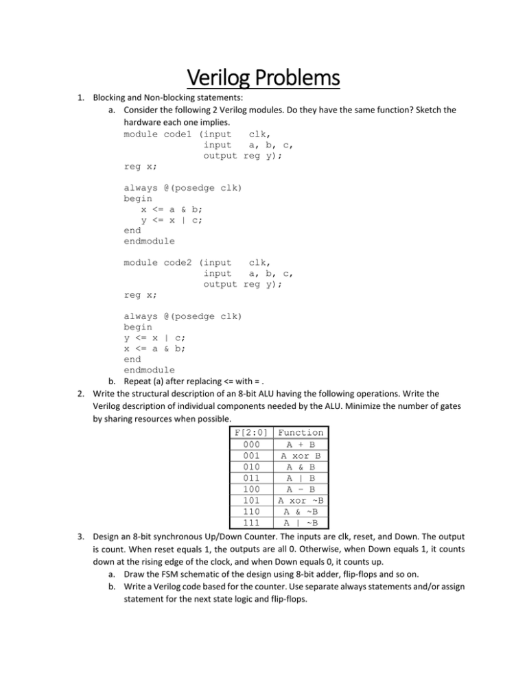
Verilog Problems 1. Blocking and Non‐blocking statements: a. Consider the following 2 Verilog modules. Do they have the same function? Sketch the hardware each one implies. module code1 (input clk, input a, b, c, output reg y); reg x; always @(posedge clk) begin x <= a & b; y <= x | c; end endmodule module code2 (input clk, input a, b, c, output reg y); reg x; always @(posedge clk) begin y <= x | c; x <= a & b; end endmodule b. Repeat (a) after replacing <= with = . 2. Write the structural description of an 8‐bit ALU having the following operations. Write the Verilog description of individual components needed by the ALU. Minimize the number of gates by sharing resources when possible. 3. Design an 8‐bit synchronous Up/Down Counter. The inputs are clk, reset, and Down. The output is count. When reset equals 1, the outputs are all 0. Otherwise, when Down equals 1, it counts down at the rising edge of the clock, and when Down equals 0, it counts up. a. Draw the FSM schematic of the design using 8‐bit adder, flip‐flops and so on. b. Write a Verilog code based for the counter. Use separate always statements and/or assign statement for the next state logic and flip‐flops. c. Write a shorter Verilog code, which is done by merging the next state logic with flip‐flops in Verilog 4. Write a Verilog description of the following: a. A magnitude comparator that compares between two 4‐bit inputs A and B and yields two outputs: A_GT_B and A_LT_B. Use continuous assignments to build the comparator. b. Use the 4‐bit comparator module developed in (a) in hierarchial fashion to build an 8‐bit magnitude comparator that compares between two 8‐bit inputs A and B and yields three outputs: A_GT_B, A_LT_B, and A_EQ_B. You can only use structural and dataflow modeling to build the comparator. c. A testbench to functionaly verify the 8‐bit comparator developed in (b). 5. Write a Verilog description of a 4-bit bidirectioanl counter module with asynchronous reset and synchronous load signal. Asserting the reset signal RST forces the output Q to 0 while asserting the load signal LD forces the output Q to the initial count D_IN. The following are the ports of the module: CLK 1-bit clock input (synchronous actions performed on rising edge) 6. 7. 8. 9. 10. RST 1-bit reset (asynchronous reset) UP_DOWN 1-bit input (if ‘1’, then count up, if ‘0’, then count down) LD 1-bit load enable input, loads synchronized with CLK rising edge D_IN 4-bit input data for loading counter value Q 4-bit output Write a verilog procedural block to swap contents of two 8-bit registers using a temporary register. Rewrite the block to swap the two registers without using a temporary register. Declare the used registers. Select signal Function Hint: Blocking Vs. Nonblocking assignments. 2’b00 OUT = A + B Using case statement, design a 4-function ALU that has 4-bit inputs 2’b01 OUT = A - B A and B and a 2-bit input select signal S, clock signal CLK, and a 5- 2’b10 OUT = A / B bit output OUT. The ALU implements functions shown in Table 2’b11 OUT = A % B based on the signal select. Ignore any overflow or underflow bits. Write the Verilog code for a negative edge triggered D flip flop with an active low asynchronous RESET. Name the module dffrn. Name the ports (in this order) Q, D, CLK, RESET. Write the full module, declaring ALL data types. Write a testbench to stimulate the dffrn module. Instantiate the module using named port mapping. You chose the period of CLK. Write the Verilog code to implement a device that will shift in serial data and increment a counter every time the pattern 16’hAFAF is found. The counter will reset every 1000 clock cycles. Assume positive edge triggered flop(s) and asynchronous active high reset. The only output of the device will be the counter. The only inputs will be data, clock, and reset. Use normal procedural statements to create the design. Consider the following Verilog module that uses Euclid’s algorithm to iteratively compute the greatest common divisor of two 16-bit unsigned integer values Ain and Bin where Ain ≥ Bin. module gcd(clk,start,Ain,Bin,answer,done); input clk,start; input [15:0] Ain,Bin; output reg [15:0] answer; output reg done; reg [15:0] a,b; always @ (posedge clk) begin if (start) begin a <= Ain; b <= Bin; done <= 0; end else if (b == 0) begin answer <= a; done <= 1; end else if (a > b) a <= a – b; else b <= b – a; end endmodule Please neatly complete the timing diagram below as the module computes the gcd of 21 and 15. Use “???” to indicate values that cannot be determined from the information given. 11. Write a Verilog description of a three-bit gray counter with positive reset. When reset, the count value becomes “000”. Recall that a Gray Counter changes only one-bit at a time. For example, a 2bit Gray counter has a count sequence 00, 01, 11, 10 corresponding to a decimal count values of 0, 1, 2, 3 respectively. In the Gray count sequence, only one bit changes between adjacent count values, and the right-most bit is changed as long as it does not result in a code word that has been visited earlier. The following are the ports of the module: CLK 1-bit clock input, all actions on positive edge RESET 1-bit reset, causes reset on positive edge GRAY_OUT 3-bit result 12. Write a Verilog description of a register that shifts data in parallel but shift data out serially, MSB first. The following are the ports of the module: CLK 1-bit clock, all operations must be on the rising edge LD 1-bit input, when high, PI is loaded into the shift register SHIFT 1-bit shift enable input, when high, contents of shift register are shifted out on to the serial output Q PI 8-bit parallel data input Q 1-bit serial output 13. Write a Verilog description of a counter that counts in both the up and down directions. The preset is to be set to decimal value 3. That is, upon asserting the reset signal low, the register value should be reset to 3. Also, upon asserting the load signal LD, the register value should be set to the input 14. 15. 16. 17. 18. value DIN. Both the reset and the load are synchronous and the module should count on the rising edge of the clock. The following are the ports of the module: CLK 1-bit clock input, all actions performed on rising edge RESET_N 1-bit preset (synchronous) UP_DNN 1-bit input (if ‘1’, then count up, if ‘0’, then count down) LD 1-bit load enable input, loads synchronized with CLK rising edge DIN 3-bit input data for loading counter value Q 3-bit result In this module, two inputs are treated as signed, 2's complement numbers and compared. The output should be a 1 if the AD_IN is greater than or equal to VS_IN. The following are the ports of the module: AD_IN 8-bit data input VS_IN 5-bit input GTE 1-bit output In this problem, you are required to model an 8-to-1 MUX with enable in Verilog, using the variety of modelling styles that the language offers (Structural, Data flow, Behavioral modeling). Complete the Verilog code for the following module header: module _8to1_MUX_struc (I, S, D, EN); input [7:0] I; input [2:0] S; input EN; output D; Design an 8-bit shifter with parallel input and output, sin_l, sin_r input lines, and shift and parallel control signals. When the shift signal is issued, data on sin_l and sin_r lines will be entered to the most and least significant bits of the register respectively, and third and fourth bits of the register will be put on a 2-bit output line named out. No shifting will be done if the unit is in parallel mode. A simple sequential multiplier is developed by adding A to itself B number of times. Both A and B inputs are 8-bit unsigned numbers. The circuit has a start input that becomes 1 for one clock when the inputs are valid. The inputs will not be valid when this signal is 0. After the start, the circuit sets its done output to 0 and starts the multiplication process. When done, it puts the result on R and sets done to 1. Given the following interface, write the complete code of this multiplier. module mult (a, b, start, clk, r, done); input [7:0] a, b; input start, clk; output [15:0] r; output done; reg [7:0] abuf, bbuf; // use these if you like reg [15:0] r; . . . endmodule Write an always statement to count the number of 1s in a given reg [255:0] InVec. Declare all necessary registers and wires. The system clock (clk) is available for you to use.


