Reduction technique for power supply noise of Analog
advertisement
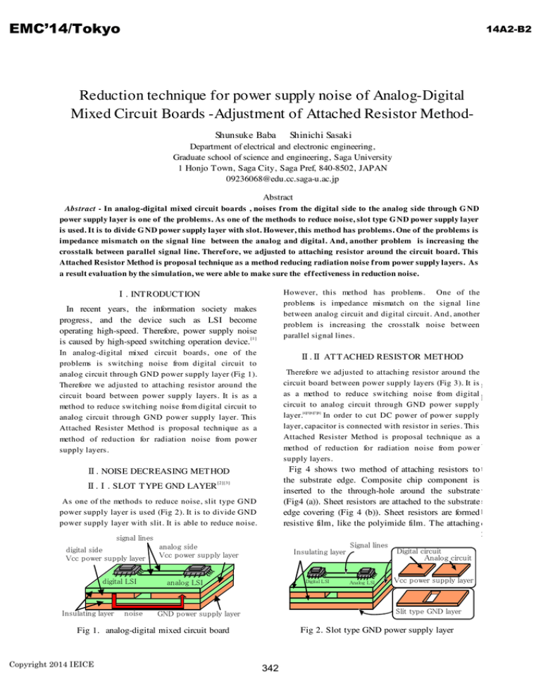
EMC’14/Tokyo 14A2-B2 Reduction technique for power supply noise of Analog-Digital Mixed Circuit Boards -Adjustment of Attached Resistor MethodShunsuke Baba Shinichi Sasaki Department of electrical and electronic engineering, Graduate school of science and engineering, Saga University 1 Honjo Town, Saga City, Saga Pref, 840-8502, JAPAN 09236068@edu.cc.saga-u.ac.jp Abstract Abstract - In analog-digital mixed circuit boards , noises f rom the digital side to the analog side through G ND power supply layer is one of the problems. As one of the methods to reduce noise, slot type G ND power supply layer is used. It is to divide G ND power supply layer with slot. However, this method has problems. One of the problems is impedance mismatch on the signal line between the analog and digital. And, another problem is increasing the crosstalk between parallel signal line. Theref ore, we adjusted to attaching resistor around the circuit board. This Attached Resistor Method is proposal technique as a method reducing radiation noise f rom power supply layers. As a result evaluation by the simulation, we were able to make sure the ef f ectiveness in reduction noise. �. INTRODUCTION However, this method has problems. One of the problems is impedance mismatch on the signal line between analog circuit and digital circuit. And, another problem is increasing the crosstalk noise between parallel signal lines. In recent years, the information society makes progress, and the device such as LSI become operating high-speed. Therefore, power supply noise [1 ] is caused by high-speed switching operation device. �.� ATTACHED RESISTOR METHOD In analog-digital mixed circuit boards, one of the problems is switching noise from digital circuit to analog circuit through GND power supply layer (Fig 1). Therefore we adjusted to attaching resistor around the circuit board between power supply layers. It is as a method to reduce switching noise from digital circuit to analog circuit through GND power supply layer. This Attached Resister Method is proposal technique as a method of reduction for radiation noise from power supply layers. Therefore we adjusted to attaching resistor around the circuit board between power supply layers (Fig 3). It is r as a method to reduce switching noise from digital p circuit to analog circuit through GND power supply layer.[4][5][6][7][8] In order to cut DC power of power supply layer, capacitor is connected with resistor in series. This Attached Resister Method is proposal technique as a method of reduction for radiation noise from power V supply layers. Fig 4 shows two method of attaching resistors to t �. NOISE DECREASING METHOD �.�. SLOT TYPE GND LAYER the substrate edge. Composite chip component is inserted to the through-hole around the substrate w (Fig4 (a)). Sheet resistors are attached to the substrate s edge covering (Fig 4 (b)). Sheet resistors are formed b resistive film, like the polyimide film. The attaching c [2 ][3 ] As one of the methods to reduce noise, slit type GND power supply layer is used (Fig 2). It is to divide GND power supply layer with slit. It is able to reduce noise. ������������ ������������� ���������������������� ����������� ���������������� ����� 2 ����������� ���������������������� ���������������� ����������� ���������� ���������� ��������������� �������������� ���������������������� ������������������� ���������������������� Fig 2. Slot type GND power supply layer Fig 1. analog-digital mixed circuit board Copyright 2014 IEICE ������������ 342 EMC’14/Tokyo ��������� 14A2-B2 ���������� �. RESULTS OF SIMULATION �������� �.�. THE EFFECT OF DECREASING OF ��� THE ATTACHING RESISTORS ���������������� ��������� Fig 3. Attached Resistor Method �������������� (resistor + capacitor) ��������� ������ (b)Chip composite component Fig 6 shows the simulation result of (a)using no resistor, (b)using slot type GND layer and (c)attaching resistors to the substrate edge. Resistors value is 53.8[ohm]. The resistors are attached on 2.5[mm] pitch. The slot is 5[mm] width in center. In the result, max noise on substrate without resistor is 6.5[V/m]. Max noise on substrate with slot type GND layer is 6.0[V/m]. Max noise on substrate with resistor is 3.5[V/m]. The smallest noise is substrate attached resistor. It was confirmed that Attached Resistor Method reduces 46.2% noise than no slit type power supply layer. �������������� ����� ������������� ���� ������ ����� (b) sheet resistor Fig 4. attached resistor method type resistance value is set the characteristic impedance of power supply layers. ��������������� ������� ������ �������������� (a) No Slit type GND power supply layer �. ANALYSIS MODEL Fig 5 shows 3D simulation model. The substrate has Vcc layer, isolation layer, GND layer. The substrate size is 100�100[mm]. The power supply layers thickness is 35[�m], the isolation layer thickness is 1.6[mm]�� Vcc layer is divided in the center 5[mm] width. Fig 5 shows simulation model structure. In simulation, We input noise to center of digital circuit between power supply layers, and measure potential charge of analog circuit . The input noise signal is 2.36[GHz] . This simulation is FDTD. ����������� 23.75�� 47.5mm Copyright 2014 IEICE ��� 2.5mm ���� ������ ��������������� �������������� (b) Slit type GND power supply layer ���� ��������� ��������������� �������������� �������������� ����������� ���������� � 50mm ��� ����� 47.5mm ����� ��������� ����������� ���� ������ ��������������� �������������� (c) No Slit type power supply layer Attached Resistor Fig 6. Simulation result 343 EMC’14/Tokyo 14A2-B2 �.�. ATTACHING POSITION For reducing resistors, we change the position of attaching resistor. Fig 7 shows four attaching positions, (Fig 7(a))digital side edge,(Fig 7(b))around digital side, (Fig 7(c))analog side edge, (Fig 7(d))around ������� analog side. (Fig 7(a)) shows simulation result of substrate attached resistor on digital side edge. In this case, max noise is 4.8[V/m]. This noise value is smaller than Fig 6(a) no resistor result. Fig 7(b) shows simulation result of substrate attached resistor around digital side. In this case, max noise is 1.7[V/m]. This noise value is a quarter of no resistor result. Fig 7(c) shows simulation result of substrate attached resistor on analog side edge. In this case, max noise is 2.7[V/m]. This noise value is smaller than Fig 6(b) slot type GND layer result. Fig 7(d) shows simulation result of substrate attached resistor around digital side. In this case, max noise is 0.9[V/m]. This noise value is the smallest in every attaching positions. In resistor position, case of attaching on analog is better for noise reduction than case of attaching on digital. It is because case of attaching on analog doesn't cause noise reflection on analog side edge. �������� ���� � ������ ����������������� �������������� (a) digital side edge ������ ������� �������� ���� ������� ����������������� �������������� (b) around�digital side ������ ������� �.�. ATTACHING RESISTOR PITCH ���� ������� �������� For reducing resistors, we change the pitch of attaching resistor. Simulation attaching position cases are five. They are digital side edge, around digital side, analog side edge, around digital side, devided ����������������� �������������� (c) analog side edge section, substrate edge. Simulation pitches of resistor are 2.5[mm], 5.0[mm], 10.0[mm], 20[mm], 50[mm]. Fig 8 shows simulation result changing pitch of attaching resistor. All of the position cases, max noise increase when attaching pitch is wide. when pitch is 2.5[mm], 5.0[mm], noise of substrate attached digital side edge is the biggest. when pitch is 2.5[mm], 5.0[mm], noise of substrate attached around analog side is the smallest. when pitch is 50[mm], noise of substrate attached all edge is the smallest. when pitch is over 10[mm], max noise of every attaching position is biger than 5[V/m]. Copyright 2014 IEICE ������ ������� s d ������ �������� ���� ������� ����������������� �������������� (d) around analog side Fig 7. Simulation result 344 f n d EMC’14/Tokyo 14A2-B2 8 ��������������������� �. CONCLUTION �� �������� 7 In this paper, I introduce the effect of.attached resistor method for analog-digital mixed circuit board. It is possible to decrease the noise on substract by attached resistor method. And it is possible to decrease the noise when resistor position and pitch. ACKNOWLEGENT 6 5 4 3 2 �������������� ����������������� 1 0 10 20 30 40 ��������������������������� In this study, we passed VLSIDesign &Education Center university of Tokyo (VDEC) . 50 8 ��� �������� 7 REFERENCES ��������������������� 6 [1]Tomoharu Okabe, Shiniti Sasaki, Shintaro Yoshimatu, "A Study of the Radiation noise Reduction Technique from P ower supply layers in the P CB", P roceedings of the IEICE General Conference, EMCJ2008-8, pp7-10 [2]Xiao Fengchao, Nakada Yohei, Murano Kimitoshi, Kami Yoshi, "Crosstalk Analysis Model for Traces Crossing Split Ground P lane and Its Reduction by Stitching Capacitor"The Transactions of the Institute of Electronics, Information and Communication Engineers C J89-C(11), 885-893, 2006-11-01. [3]Hirayama Hiroshi, Kami Yoshio, "Slot-line model for the slit on a ground plane and its limitation",IEICE technical report. Electromagnetic compatibility 103(488), 35-40, 2003-11-28 [4]Tomoharu Okabe, Shiniti Sasaki, Shintaro Yoshimatu, "Examination of Reduction Technique for Radiation noisefrom the P ower supply layers to P CB", The 62th Joint Conference of Electrical and Electrics in Kyushu, 11-1A-09, 2008 [5]Shunsuke Baba, Shiniti Sasaki, Hitoshi Takakura, Hiroaki Matsumoto"Reduction technique for power supply noise of Analog-Digital Mixed Circuit Boards - Adjustment of Attached Resistor Method -" [6]Shiniti Sasaki, Tomoharu Okabe, "Examination of Reduction Technique for Radiation noisefrom the P ower supply layers to P CB", P roceeding of the 23rd JIEP Annual Meeting March, 2009, pp127-128 [7]Hitoshi Takakura, Shinichi Sasaki, Tomoharu Okabe, "Examination of Reduction Technique for Radiation noise from the P ower supply layers in P CB : P ower supply layers edge geometry", IEICE technical report. Electromagnetic compatibility 109(370), 87-91, 2010-01-14 5 4 3 2 �������������� ������������� 1 ���������������� 0 0 10 20 30 40 50 ��������������������������� Fig 8. effect of resistor pitch �.�. RADIATION NOISE Fig 6 shows the simulation result of radiation noise from substrate. This shows four attaching positions, no resistor, digital side edge,digital side edge and divided section and substrate edge. In this figure, attaching resistor position of the smollest radiation noise is digital side edge and divided section. -25 ������������� ���� ����������� -30 -35 -40 -45 -50 -55 -60 -65 �������������� ������������������ ������������ �������� -70 Fig 9. radiation noise Copyright 2014 IEICE 345
