Lab # 7 - Rose
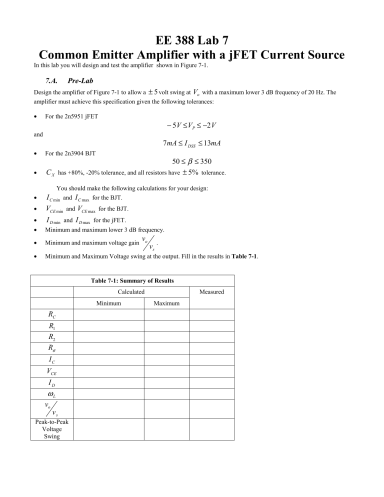
R
C
R
1
R
2
R
σ
I
C
V
CE
I
D
ω
L v o v s
Peak-to-Peak
Voltage
Swing
7. Common Emitter Amplifier with a jFET Current Source
EE 388 Lab 7
Common Emitter Amplifier with a jFET Current Source
In this lab you will design and test the amplifier shown in Figure 7-1.
7.A. Pre-Lab
Design the amplifier of Figure 7-1 to allow a
±
5 volt swing at V o
with a maximum lower 3 dB frequency of 20 Hz. The
amplifier must achieve this specification given the following tolerances:
• For the 2n5951 jFET
−
5 V
≤
V
P
≤
V and
−
2
7 mA
≤
I
DSS
≤
13 mA
• For the 2n3904 BJT
•
50
≤ β ≤
350
C
X
has +80%, -20% tolerance, and all resistors have
±
5 % tolerance.
•
You should make the following calculations for your design:
I
C min
and I
C max
for the BJT.
• V
CE min
and V
CE max
for the BJT.
• I
D min
and I
D max
for the jFET.
• Minimum and maximum lower 3 dB frequency.
• Minimum and maximum voltage gain v o v s
.
• Minimum and Maximum Voltage swing at the output. Fill in the results in Table 7-1 .
Table 7-1: Summary of Results
Minimum Maximum
7.B.1. Bias Measurements
The first thing you should do on any amplifier is check the bias of the circuit. If the bias does not work, nothing else will.
When you check the bias you must set all ac sources to zero. This is accomplished by grounding the base of the BJT as shown in Figure 7-2 . Measure the bias and fill in Table 7-1 . If your measured values do not fall within the minimum and maximum calculated values check your circuit or your calculations.
7.B.2. AC Measurements
Once the bias is correct, measure the midland voltage gain, maximum peak-peak output voltage swing, and lower 3 dB frequency. Remember that gain and bandwidth must be measured using small signal waveforms.
Vcc=15V
-
+
Vs
Rc
Q1
Q2N3904
Vo
Cx
R1
R2
J1
J2n5951
Rs
-Vee=-15V
Figure 7-1 : Common-emitter amplifier with a jFET current source for the bias.
Vcc=15V
Rc
Q1
Q2N3904
Vo
Cx
R1
R2
J1
J2n5951
Rs
-Vee=-15V
Figure 7-2 : Common-emitter amplifier with a jFET current source for the bias.The input is grounded to measure the bias.
