CMPA801B025
25 W, 8.5 - 11.0 GHz, GaN MMIC, Power Amplifier
Cree’s CMPA801B025 is a gallium nitride (GaN) High Electron Mobility
Transistor (HEMT) based monolithic microwave integrated circuit (MMIC).
GaN has superior properties compared to silicon or gallium arsenide, including
higher breakdown voltage, higher saturated electron drift velocity and higher
thermal conductivity. GaN HEMTs also offer greater power density and wider
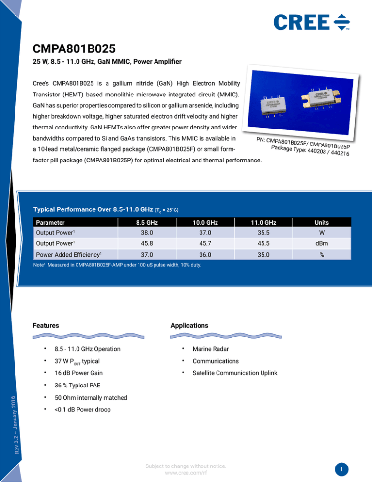
bandwidths compared to Si and GaAs transistors. This MMIC is available in
a 10-lead metal/ceramic flanged package (CMPA801B025F) or small form-
PN: CMPA801B
025F/ CMPA80
1B025P
Package Type
: 440208 / 44
0216
factor pill package (CMPA801B025P) for optimal electrical and thermal performance.
Typical Performance Over 8.5-11.0 GHz (TC = 25˚C)
Parameter
Output Power
1
Output Power1
Power Added Efficiency
1
8.5 GHz
10.0 GHz
11.0 GHz
Units
38.0
37.0
35.5
W
45.8
45.7
45.5
dBm
37.0
36.0
35.0
%
Note : Measured in CMPA801B025F-AMP under 100 uS pulse width, 10% duty.
1
Features
Applications
• 8.5 - 11.0 GHz Operation
• Marine Radar
• 37 W POUT typical
• Communications
• 16 dB Power Gain
• Satellite Communication Uplink
ary
Rev 3.2 – Janu
2016
• 36 % Typical PAE
• 50 Ohm internally matched
• <0.1 dB Power droop
Subject to change without notice.
www.cree.com/rf
1
Absolute Maximum Ratings (not simultaneous)
Parameter
Symbol
Rating
Units
Conditions
Drain-source Voltage
VDSS
84
VDC
25˚C
Gate-source Voltage
VGS
-10, +2
VDC
25˚C
Power Dissipation
PDISS
77
W
Storage Temperature
TSTG
-55, +150
˚C
Operating Junction Temperature
TJ
225
˚C
Maximum Forward Gate Current
IGMAX
13
mA
Soldering Temperature1
TS
245
˚C
25˚C
Screw Torque
τ
40
in-oz
Thermal Resistance, Junction to Case
RθJC
1.22
˚C/W
Pulse Width = 100 µs, Duty Cycle = 10%, PDISS = 55 W
Thermal Resistance, Junction to Case
RθJC
1.80
˚C/W
CW, PDISS = 55 W, 85˚C
Case Operating Temperature
TC
-40, +130
˚C
Pulse Width = 100 µs, Duty Cycle = 10%, PDISS = 55 W
Case Operating Temperature
TC
-40, +90
˚C
CW, PDISS = 55 W
Note:
1
Refer to the Application Note on soldering at www.cree.com/RF/Document-Library
Electrical Characteristics (Frequency = 8.5 GHz to 11.0 GHz unless otherwise stated; TC = 25˚C)
Characteristics
Symbol
Min.
Typ.
Max.
Units
VGS(TH)
-3.8
-3.0
-2.3
V
VDS = 10 V, ID = 13.2 mA
Gate Quiscent Voltage
VQ
–
-2.7
–
V
VDS = 28 V, ID = 1.2 A
Saturated Drain Current2
IDS
10.6
13.0
–
A
VDS = 6.0 V, VGS = 2.0 V
Drain-Source Breakdown Voltage
VBD
84
100
–
V
VGS = -8 V, ID = 13.2 mA
Small Signal Gain
S21
20
24
–
dB
Input Return Loss
S11
–
–6.0
–
dB
VDD = 28 V, IDQ = 1.2 A
Output Return Loss
S22
–
–6.0
–
dB
VDD = 28 V, IDQ = 1.2 A
DC Characteristics
Gate Threshold
RF Characteristics
Conditions
1
3
VDD = 28 V, IDQ = 1.2 A,
PIN = -20 dBm
No damage at all phase angles, VDD =
Output Mismatch Stress
VSWR
–
–
5:1
Y
28 V, IDQ = 1.2 A,
Pulse Width = 100 µs, Duty Cycle =
10%, PIN = 30 dBm
Notes:
1
Measured on-wafer prior to packaging.
2
Scaled from PCM data.
3
Measured in the CMPA801B025F-AMP.
Copyright © 2011-2016 Cree, Inc. All rights reserved. The information in this document is subject to change without notice. Cree and the Cree logo are
registered trademarks of Cree, Inc. Other trademarks, product and company names are the property of their respective owners and do not imply specific
product and/or vendor endorsement, sponsorship or association.
2
CMPA801B025 Rev 3.2
Cree, Inc.
4600 Silicon Drive
Durham, North Carolina, USA 27703
USA Tel: +1.919.313.5300
Fax: +1.919.869.2733
www.cree.com/rf
Electrical Characteristics Continued... (TC = 25˚C)
Characteristics
Symbol
Min.
Typ.
Max.
Units
Conditions
Output Power
POUT1
44.75
45.8
–
dBm
VDD = 28 V, IDQ = 1.2 A, Frequency = 8.5 GHz, PIN = 30 dBm
Output Power
POUT2
44.75
45.7
–
dBm
VDD = 28 V, IDQ = 1.2 A, Frequency = 10.0 GHz, PIN = 30 dBm
Output Power
POUT3
44.35
45.5
–
dBm
VDD = 28 V, IDQ = 1.2 A, Frequency = 11.0 GHz, PIN = 30 dBm
Power Gain
G1
14.75
15.8
–
dB
VDD = 28 V, IDQ = 1.2 A, Frequency = 8.5 GHz, PIN = 30 dBm
Power Gain
G2
14.75
15.7
–
dB
VDD = 28 V, IDQ = 1.2 A, Frequency = 10.0 GHz, PIN = 30 dBm
Power Gain
G3
14.35
15.5
–
dB
VDD = 28 V, IDQ = 1.2 A, Frequency = 11.0 GHz, PIN = 30 dBm
Power Added Efficiency
PAE1
29
37
–
%
VDD = 28 V, IDQ = 1.2 A, Frequency = 8.5 GHz, PIN = 30 dBm
Power Added Efficiency
PAE2
29
36
–
%
VDD = 28 V, IDQ = 1.2 A, Frequency = 10.0 GHz, PIN = 30 dBm
Power Added Efficiency
PAE3
27
35
–
%
VDD = 28 V, IDQ = 1.2 A, Frequency = 11.0 GHz, PIN = 30 dBm
Pulse Amplitude Droop
D
–
0.1
–
dB
VDD = 28 V, IDQ = 1.2 A, Frequency = 8.5 - 11.0 GHz, PIN = 30 dBm
RF Characteristics1,2
Notes:
1
Pulse Width = 100 μS, Duty Cycle = 10 %.
2
Measured in CMPA801B025F-AMP.
Electrostatic Discharge (ESD) Classifications
Parameter
Symbol
Class
Test Methodology
Human Body Model
HBM
1A (> 250 V)
JEDEC JESD22 A114-D
Charge Device Model
CDM
II (200 < 500 V)
JEDEC JESD22 C101-C
Copyright © 2011-2016 Cree, Inc. All rights reserved. The information in this document is subject to change without notice. Cree and the Cree logo are
registered trademarks of Cree, Inc. Other trademarks, product and company names are the property of their respective owners and do not imply specific
product and/or vendor endorsement, sponsorship or association.
3
CMPA801B025 Rev 3.2
Cree, Inc.
4600 Silicon Drive
Durham, North Carolina, USA 27703
USA Tel: +1.919.313.5300
Fax: +1.919.869.2733
www.cree.com/rf
CMPA801B025F Typical Performance
50
50%
45
45%
40
40%
35
35%
30
30%
25
25%
20
20%
15
15%
10
5
0
7500
Output Power (W)
10%
Gain (dB)
Output Power (dBm)
5%
PAE (%)
8000
8500
Efficiency (%)
Power (W, dBm) Gain (dB)
Figure 1. - Output Power, Gain and Power Added Efficiency vs. Frequency
VDD = 28 V, PIN = 30 dBm, IDQ = 1.2 A
Pulsed
data
100uS 10%
Vdd=28v
Pin=30dBm
Idq=1200mA
Pulse Width
= 100
μS, Duty
Cycle = 10
%
9000
9500
10000
Frequency (MHz)
10500
11000
0%
11500
50
50%
45
45%
40
40%
35
35%
30
30%
25
25%
20
20%
15
15%
10
5
0
7500
10%
CW Psat Power (W)
CW Psat Power (dBm)
CW Psat Gain (dB)
CW Psat PAE (%)
8000
8500
5%
9000
9500
10000
Frequency (MHz)
10500
11000
Copyright © 2011-2016 Cree, Inc. All rights reserved. The information in this document is subject to change without notice. Cree and the Cree logo are
registered trademarks of Cree, Inc. Other trademarks, product and company names are the property of their respective owners and do not imply specific
product and/or vendor endorsement, sponsorship or association.
4
CMPA801B025 Rev 3.2
Efficiency (%)
Power (W, dBm) Gain (dB)
Figure 2. - Output Power, Gain and Power Added Efficiency vs. Frequency
VDD =
28Psat
V, I(Ig≈1.5mA)
= 1.2 A,Vd=28V
CW PSAT
(IG ≈ 1.5mA)
CW
Idq=1200mA
DQ
0%
11500
Cree, Inc.
4600 Silicon Drive
Durham, North Carolina, USA 27703
USA Tel: +1.919.313.5300
Fax: +1.919.869.2733
www.cree.com/rf
CMPA801B025F Typical Performance
50%
45
45%
40
40%
35
35%
30
30%
25
25%
20
20%
15
15%
Output Power (dBm)
10
10%
Output Power (W)
Gain (dB)
5
Efficiency %
Power (W, dBm) Gain (dB)
50
Figure 3. - Output Power, Gain and Power Added Efficiency vs. Input Power
VDD = 28 V, IDQ = 1.2 A, Frequency = 11 GHz
5%
PAE %
0%
0
16
18
20
22
24
26
28
30
32
Input Power (dBm)
Figure 4. -Small
SmallSignal
SignalS-Parameters
S-Parameters
Frequency
vs. vs.
Frequency
30
S11 (dB), S21 (dB), S22 (dB)
20
10
0
-10
-20
S(2,1)
S(1,1)
-30
6000
S(2,2)
7000
8000
9000
10000
11000
12000
Frequency (MHz)
Copyright © 2011-2016 Cree, Inc. All rights reserved. The information in this document is subject to change without notice. Cree and the Cree logo are
registered trademarks of Cree, Inc. Other trademarks, product and company names are the property of their respective owners and do not imply specific
product and/or vendor endorsement, sponsorship or association.
5
CMPA801B025 Rev 3.2
Cree, Inc.
4600 Silicon Drive
Durham, North Carolina, USA 27703
USA Tel: +1.919.313.5300
Fax: +1.919.869.2733
www.cree.com/rf
CMPA801B025F Typical Performance
Figure
5. - Power
Dissipation
CMPA801B025F
Power
DissipationDerating
De-Rating Curve
Curve
90
80
Power Dissipation (W)
70
60
50
40
Note 1
Derating Curve Pulsed 10% 100uS
30
Derating Curve CW
`
20
10
0
0
25
50
75
100
125
150
Maximum Case Temperature ( C)
175
200
225
250
Note 1. Area exceeds Maximum Case Operating Temperature (See Page 2).
Copyright © 2011-2016 Cree, Inc. All rights reserved. The information in this document is subject to change without notice. Cree and the Cree logo are
registered trademarks of Cree, Inc. Other trademarks, product and company names are the property of their respective owners and do not imply specific
product and/or vendor endorsement, sponsorship or association.
6
CMPA801B025 Rev 3.2
Cree, Inc.
4600 Silicon Drive
Durham, North Carolina, USA 27703
USA Tel: +1.919.313.5300
Fax: +1.919.869.2733
www.cree.com/rf
CMPA801B025F-AMP Demonstration Amplifier Circuit Bill of Materials
Designator
C15
Description
Qty
CAP ELECT 100UF 80V AFK SMD
1
RES 0.0 OHM 1/16W 0402 SMD
2
W1
WIRE, BLACK, 22 AWG ~ 1.50”
1
W2
WIRE, BLACK, 22 AWG ~ 1.75”
1
W3
WIRE, BLACK, 22 AWG ~ 2.0”
1
CONNECTOR, SMA, PANEL MOUNT JACK, FLANGE,
4-HOLE, BLUNT POST, 20MIL
2
J3
CONNECTOR, HEADER, RT>PLZ .1CEN LK 9POS
1
J4
CONNECTOR, SMB-U SURFACE MOUNT
1
-
PCB, TEST FIXTURE, TACONICS RF35P, 20 MILS,
440208 PKG
1
-
2-56 SOC HD SCREW 1/4 SS
4
-
#2 SPLIT LOCKWASHER SS
4
CMPA801B025F
1
R1, R2
J1,J2
Q1
CMPA801B025F-AMP Demonstration Amplifier Circuit
Copyright © 2011-2016 Cree, Inc. All rights reserved. The information in this document is subject to change without notice. Cree and the Cree logo are
registered trademarks of Cree, Inc. Other trademarks, product and company names are the property of their respective owners and do not imply specific
product and/or vendor endorsement, sponsorship or association.
7
CMPA801B025 Rev 3.2
Cree, Inc.
4600 Silicon Drive
Durham, North Carolina, USA 27703
USA Tel: +1.919.313.5300
Fax: +1.919.869.2733
www.cree.com/rf
CMPA801B025F-AMP Demonstration Amplifier Circuit Schematic
CMPA801B025F-AMP Demonstration Amplifier Circuit Outline
Copyright © 2011-2016 Cree, Inc. All rights reserved. The information in this document is subject to change without notice. Cree and the Cree logo are
registered trademarks of Cree, Inc. Other trademarks, product and company names are the property of their respective owners and do not imply specific
product and/or vendor endorsement, sponsorship or association.
8
CMPA801B025 Rev 3.2
Cree, Inc.
4600 Silicon Drive
Durham, North Carolina, USA 27703
USA Tel: +1.919.313.5300
Fax: +1.919.869.2733
www.cree.com/rf
CMPA801B025F-AMP Demonstration Amplifier Circuit Schematic
To configure the CMPA801B025F test fixture to enable independent VG1 / VG2 control of the device, a cut
must be made to the microstrip line just above the R1 resistor as shown. Pin 9 will then supply VG1 and Pin 8 will
supply VG2.
CMPA801B025F Typical Performance
ThetaJC (⁰C/W)
Figure 7. - Transient Thermal Performance
TCASE
85°C
X-Band MMIC on 440208 Pkg, .25"
Thk=Cu
Fixture, Tcase=85⁰C
1.90
1.85
1.80
1.75
1.70
1.65
1.60
1.55
1.50
1.45
1.40
1.35
1.30
1.25
1.20
1.15
1.10
1.05
1.00
0.95
0.90
0.85
0.80
0.75
0.70
0.65
0.60
0.55
0.50
1.00E-06
10% Duty Cycle
20% Duty Cycle
50% Duty Cycle
1.00E-05
1.00E-04
1.00E-03
Time (seconds)
1.00E-02
1.00E-01
Copyright © 2011-2016 Cree, Inc. All rights reserved. The information in this document is subject to change without notice. Cree and the Cree logo are
registered trademarks of Cree, Inc. Other trademarks, product and company names are the property of their respective owners and do not imply specific
product and/or vendor endorsement, sponsorship or association.
9
CMPA801B025 Rev 3.2
1.00E+00
Cree, Inc.
4600 Silicon Drive
Durham, North Carolina, USA 27703
USA Tel: +1.919.313.5300
Fax: +1.919.869.2733
www.cree.com/rf
Product Dimensions CMPA801B025F (Package Type —
­ 440208)
Pin Number
Qty
1
Gate Bias for Stage 2
2
Gate Bias for Stage 2
3
RF In
4
Gate Bias for Stage 1
5
Gate Bias for Stage 1
6
Drain Bias
7
Drain Bias
8
RF Out
9
Drain Bias
10
Drain Bias
11
Source
Copyright © 2011-2016 Cree, Inc. All rights reserved. The information in this document is subject to change without notice. Cree and the Cree logo are
registered trademarks of Cree, Inc. Other trademarks, product and company names are the property of their respective owners and do not imply specific
product and/or vendor endorsement, sponsorship or association.
10
CMPA801B025 Rev 3.2
Cree, Inc.
4600 Silicon Drive
Durham, North Carolina, USA 27703
USA Tel: +1.919.313.5300
Fax: +1.919.869.2733
www.cree.com/rf
Product Dimensions CMPA801B025P (Package Type —
­ 440216)
Pin Number
Qty
1
Gate Bias for Stage 2
2
Gate Bias for Stage 2
3
RF In
4
Gate Bias for Stage 1
5
Gate Bias for Stage 1
6
Drain Bias
7
Drain Bias
8
RF Out
9
Drain Bias
10
Drain Bias
11
Source
Copyright © 2011-2016 Cree, Inc. All rights reserved. The information in this document is subject to change without notice. Cree and the Cree logo are
registered trademarks of Cree, Inc. Other trademarks, product and company names are the property of their respective owners and do not imply specific
product and/or vendor endorsement, sponsorship or association.
11
CMPA801B025 Rev 3.2
Cree, Inc.
4600 Silicon Drive
Durham, North Carolina, USA 27703
USA Tel: +1.919.313.5300
Fax: +1.919.869.2733
www.cree.com/rf
Part Number System
CMPA801B025F
Package
Power Output (W)
Upper Frequency (GHz)
Lower Frequency (GHz)
Cree MMIC Power Amplifier Product Line
Parameter
Value
Units
Lower Frequency
8.5
GHz
Upper Frequency1
11.0
GHz
25
W
Flange
-
Power Output
Package
Table 1.
Note : Alpha characters used in frequency code
1
indicate a value greater than 9.9 GHz. See Table
2 for value.
Character Code
Code Value
A
0
B
1
C
2
D
3
E
4
F
5
G
6
H
7
J
8
K
9
Examples:
1A = 10.0 GHz
2H = 27.0 GHz
Table 2.
Copyright © 2011-2016 Cree, Inc. All rights reserved. The information in this document is subject to change without notice. Cree and the Cree logo are
registered trademarks of Cree, Inc. Other trademarks, product and company names are the property of their respective owners and do not imply specific
product and/or vendor endorsement, sponsorship or association.
12
CMPA801B025 Rev 3.2
Cree, Inc.
4600 Silicon Drive
Durham, North Carolina, USA 27703
USA Tel: +1.919.313.5300
Fax: +1.919.869.2733
www.cree.com/rf
Product Ordering Information
Order Number
Description
Unit of Measure
CMPA801B025F
GaN HEMT
Each
CMPA801B025P
GaN HEMT
Each
Test board without GaN HEMT
Each
Test board with GaN HEMT installed
Each
CMPA801B025F-TB
CMPA801B025F-AMP
Copyright © 2011-2016 Cree, Inc. All rights reserved. The information in this document is subject to change without notice. Cree and the Cree logo are
registered trademarks of Cree, Inc. Other trademarks, product and company names are the property of their respective owners and do not imply specific
product and/or vendor endorsement, sponsorship or association.
13
CMPA801B025 Rev 3.2
Image
Cree, Inc.
4600 Silicon Drive
Durham, North Carolina, USA 27703
USA Tel: +1.919.313.5300
Fax: +1.919.869.2733
www.cree.com/rf
Disclaimer
Specifications are subject to change without notice. Cree, Inc. believes the information contained within this data sheet to be accurate
and reliable. However, no responsibility is assumed by Cree for its use or for any infringement of patents or other rights of third parties
which may result from its use. No license is granted by implication or otherwise under any patent or patent rights of Cree. Cree makes
no warranty, representation or guarantee regarding the suitability of its products for any particular purpose. “Typical” parameters are the
average values expected by Cree in large quantities and are provided for information purposes only. These values can and do vary in
different applications, and actual performance can vary over time. All operating parameters should be validated by customer’s technical
experts for each application. Cree products are not designed, intended, or authorized for use as components in applications intended for
surgical implant into the body or to support or sustain life, in applications in which the failure of the Cree product could result in personal
injury or death, or in applications for the planning, construction, maintenance or direct operation of a nuclear facility. CREE and the CREE
logo are registered trademarks of Cree, Inc.
For more information, please contact:
Cree, Inc.
4600 Silicon Drive
Durham, North Carolina, USA 27703
www.cree.com/RF
Sarah Miller
Marketing
Cree, RF Components
1.919.407.5302
Ryan Baker
Marketing & Sales
Cree, RF Components
1.919.407.7816
Tom Dekker
Sales Director
Cree, RF Components
1.919.407.5639
Copyright © 2011-2016 Cree, Inc. All rights reserved. The information in this document is subject to change without notice. Cree and the Cree logo are
registered trademarks of Cree, Inc. Other trademarks, product and company names are the property of their respective owners and do not imply specific
product and/or vendor endorsement, sponsorship or association.
14
CMPA801B025 Rev 3.2
Cree, Inc.
4600 Silicon Drive
Durham, North Carolina, USA 27703
USA Tel: +1.919.313.5300
Fax: +1.919.869.2733
www.cree.com/rf


