Evaluation Board User Guide
UG-044
One Technology Way • P.O. Box 9106 • Norwood, MA 02062-9106, U.S.A. • Tel: 781.329.4700 • Fax: 781.461.3113 • www.analog.com
Evaluating the ADM2582E/ADM2587E
FEATURES
The board can be easily configured by jumper connections.
The board is configurable as half-duplex or full-duplex and
has a 120 Ω termination resistor fitted on the receiver input.
The evaluation board can be used with both the ADM2582E
16 Mbps part and the ADM2587E 500 kbps part. The driver
and receiver can be enabled and disabled by jumper connections.
Test points are included on the power and signal lines on both
sides of the isolation barrier.
Power and signal isolated RS-485/RS422 transceiver
Convenient connections for power and signal through screw
terminal blocks
Configurable as half-duplex or full-duplex
5 V or 3.3 V operation
Easily configurable through jumper connections
Test points for measuring all signals
Layout optimized for emissions according to the AN-0971
Application Note
Passes the EN55022(2001) Class B emissions standard
RADIATED EMISSIONS
The ADM2582E/ADM2587E evaluation board is designed to
reduce emissions generated by the high frequency switching
elements used by the isoPower technology to transfer power
through its transformer. Guidelines mentioned in the AN-0971
Application Note were used to generate the layout. The emissions
of the evaluation board were measured by an independent test
facility and passed the EN55022(2001) Class B emissions standard.
GENERAL DESCRIPTION
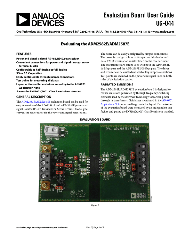
The ADM2582E/ADM2587E evaluation board can be used for
easy evaluation of the ADM2582E and ADM2587E power and
signal isolated RS-485 transceivers. Screw terminal blocks give
convenient connections for the power and signal connections.
08420-001
EVALUATION BOARD
Figure 1.
See the last page for an important warning and disclaimers.
Rev. 0 | Page 1 of 8
UG-044
Evaluation Board User Guide
TABLE OF CONTENTS
Features .............................................................................................. 1
Assembly Drawings and Board Layout ..........................................4
General Description ......................................................................... 1
Hardware Configuration ..................................................................7
Radiated Emissions .......................................................................... 1
Evaluation Board Jumper Settings ..............................................7
Evaluation Board .............................................................................. 1
Decoupling and Reservoir Capacitors ........................................8
Revision History ............................................................................... 2
Board Internal Layer Thickness ..................................................8
Evaluation Board Schematics .......................................................... 3
ESD Caution .......................................................................................8
REVISION HISTORY
11/09—Revision 0: Initial Version
Rev. 0 | Page 2 of 8
Evaluation Board User Guide
UG-044
EVALUATION BOARD SCHEMATICS
08420-002
Figure 2. Schematic of the ADM2582E/ADM2587E Evaluation Board
Rev. 0 | Page 3 of 8
UG-044
Evaluation Board User Guide
08420-003
ASSEMBLY DRAWINGS AND BOARD LAYOUT
08420-004
Figure 3. Top Layer
08420-005
Figure 4. Silkscreen
Figure 5. Internal Layer 2
Rev. 0 | Page 4 of 8
UG-044
08420-006
Evaluation Board User Guide
08420-007
Figure 6. Internal Layer 3
08420-008
Figure 7. Internal Layer 4
Figure 8. Internal Layer 5
Rev. 0 | Page 5 of 8
Evaluation Board User Guide
08420-009
UG-044
Figure 9. Bottom Solder Layer
Rev. 0 | Page 6 of 8
Evaluation Board User Guide
UG-044
HARDWARE CONFIGURATION
EVALUATION BOARD JUMPER SETTINGS
Table 1.
Link
LK1
Connection
A
Description
Connects the receiver output (RxD) of the ADM2582E/ADM2587E to the J3 connector.
LK1
B
Connects the receiver output (RxD) of the ADM2582E/ADM2587E to the J8-1 terminal block connector.
A
B
LK2
A
Connects the receiver enable input (RE) of the ADM2582E/ADM2587E to VCC. This disables the receiver.
A
B
C
LK2
B
Connects the receiver enable input (RE) of the ADM2582E/ADM2587E to GND1. This enables the receiver.
A
B
C
LK2
C
A
B
C
LK3
A
Connects the receiver enable input (RE) of the ADM2582E/ADM2587E to the J8-2 terminal block
connector.
Connects the driver enable input (DE) of the ADM2582E/ADM2587E to VCC. This enables the driver.
LK3
B
Connects the driver enable input (DE) of the ADM2582E/ADM2587E to GND1. This disables the driver.
A
B
C
LK3
C
Connects the driver enable input (DE) of the ADM2582E/ADM2587E to the J8-3 terminal block
connector.
A
B
C
LK4
A
Connects the receiver output (RxD) of the ADM2582E/ADM2587E to the J8-4 connector.
A
B
LK4
B
Connects the receiver output (RxD) of the ADM2582E/ADM2587E to the J2 terminal block connector.
A
B
LK5
Connected
LK5
LK5
LK6
Open
Connected
LK6
LK14
Open
Connected
LK14
Open
Connects the ADM2582E/ADM2587E Receiver Input B to Driver Output Z. When LK5 and LK6 are both
connected, the evaluation board is connected in a half-duplex configuration.
When LK5 and LK6 are both open, the evaluation board is connected in a full-duplex configuration.
Connects the ADM2582E/ADM2587E Receiver Input A to Driver Output Y. When LK5 and LK6 are both
connected, the evaluation board is connected in a half-duplex configuration.
When LK5 and LK6 are both open, the evaluation board is connected in a full-duplex configuration.
Connects the driver enable input (DE) of the ADM2582E/ADM2587E to the receiver enable input
(RE) of the ADM2582E/ADM2587E. This ensures that, when the driver is enabled, the receiver is disabled
or that, when the driver is disabled, the receiver is enabled.
Disconnects the driver enable input (DE) of the ADM2582E/ADM2587E from the receiver input enable
(RE) of the ADM2582E/ADM2587E.
Rev. 0 | Page 7 of 8
Image
A
B
A
B
C
LK5
LK6
LK6
LK14
LK14
UG-044
Evaluation Board User Guide
DECOUPLING AND RESERVOIR CAPACITORS
Table 2.
On the logic side of the board, the C4 and C6 capacitors should
be 10 µF and 100 nF ceramic capacitors, and the C2 and C1
capacitors should be 100 nF and 10 nF ceramic capacitors. On
the bus side of the board, the C5 and C8 capacitors should be
100 nF and 10 µF, and the C9 and C7 capacitors should be 10 nF
and 100 nF.
Layers
1 to 2
2 to 3
3 to 4
4 to 5
5 to 6
Thickness (mm) of Space Between Layers
0.1016
0.2032
0.2032
0.2032
0.1016
BOARD INTERNAL LAYER THICKNESS
The ADM2582E/ADM2587E evaluation board consists of six
internal layers. The spacing between the internal board layers
was chosen to maximize the stitching capacitance on the board.
ESD CAUTION
Evaluation boards are only intended for device evaluation and not for production purposes. Evaluation boards are supplied “as is” and without warranties of any kind, express,
implied, or statutory including, but not limited to, any implied warranty of merchantability or fitness for a particular purpose. No license is granted by implication or otherwise under
any patents or other intellectual property by application or use of evaluation boards. Information furnished by Analog Devices is believed to be accurate and reliable. However, no
responsibility is assumed by Analog Devices for its use, nor for any infringements of patents or other rights of third parties that may result from its use. Analog Devices reserves the
right to change devices or specifications at any time without notice. Trademarks and registered trademarks are the property of their respective owners. Evaluation boards are not
authorized to be used in life support devices or systems.
©2009 Analog Devices, Inc. All rights reserved. Trademarks and
registered trademarks are the property of their respective owners.
UG08420-0-11/09(0)
Rev. 0 | Page 8 of 8


