MP3302
40V, 1.3A, Single-cell Step-up
White LED Driver
with Single Wire Dimming Control
The Future of Analog IC Technology
DESCRIPTION
FEATURES
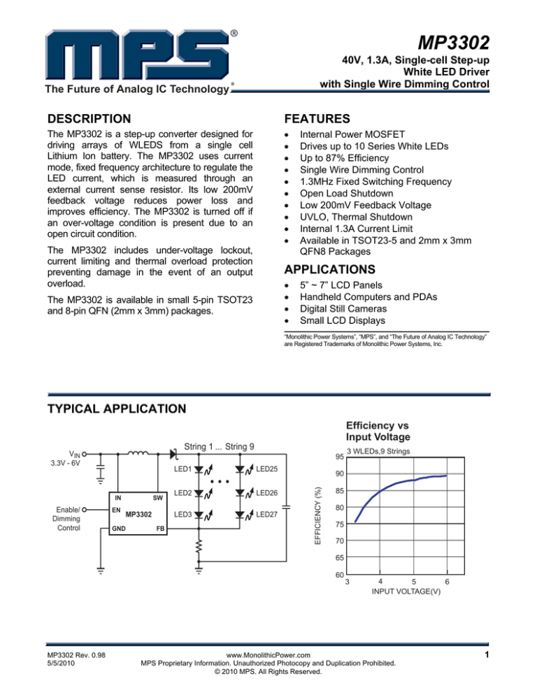
The MP3302 is a step-up converter designed for
driving arrays of WLEDS from a single cell
Lithium Ion battery. The MP3302 uses current
mode, fixed frequency architecture to regulate the
LED current, which is measured through an
external current sense resistor. Its low 200mV
feedback voltage reduces power loss and
improves efficiency. The MP3302 is turned off if
an over-voltage condition is present due to an
open circuit condition.
•
•
•
•
•
•
•
•
•
•
The MP3302 includes under-voltage lockout,
current limiting and thermal overload protection
preventing damage in the event of an output
overload.
Internal Power MOSFET
Drives up to 10 Series White LEDs
Up to 87% Efficiency
Single Wire Dimming Control
1.3MHz Fixed Switching Frequency
Open Load Shutdown
Low 200mV Feedback Voltage
UVLO, Thermal Shutdown
Internal 1.3A Current Limit
Available in TSOT23-5 and 2mm x 3mm
QFN8 Packages
APPLICATIONS
•
•
•
•
The MP3302 is available in small 5-pin TSOT23
and 8-pin QFN (2mm x 3mm) packages.
5” ~ 7” LCD Panels
Handheld Computers and PDAs
Digital Still Cameras
Small LCD Displays
“Monolithic Power Systems”, “MPS”, and “The Future of Analog IC Technology”
are Registered Trademarks of Monolithic Power Systems, Inc.
TYPICAL APPLICATION
String 1 ... String 9
VIN
3.3V - 6V
95
EN
SW
MP3302
GND
FB
LED1
LED25
LED2
LED26
LED3
LED27
3 WLEDs,9 Strings
90
EFFICIENCY (%)
IN
Enable/
Dimming
Control
Efficiency vs
Input Voltage
85
80
75
70
65
60
MP3302 Rev. 0.98
5/5/2010
3
4
5
6
INPUT VOLTAGE(V)
www.MonolithicPower.com
MPS Proprietary Information. Unauthorized Photocopy and Duplication Prohibited.
© 2010 MPS. All Rights Reserved.
1
MP3302 –40V, 1.3A, SINGLE-CELL STEP-UP WHITE LED DRIVER WITH SINGLE WIRE DIMMING CONTROL
ORDERING INFORMATION
Part Number
MP3302DJ*
MP3302DD**
Package
TSOT23-5
QFN8 (2mm x 3mm)
Top Marking
N6
N7
Free Air Temperature (TA)
–40°C to +85°C
–40°C to +85°C
* For Tape & Reel, add suffix –Z (e.g. MP3302DJ–Z);
For RoHS Compliant Packaging, add suffix –LF (e.g. MP3302DJ–LF–Z).
** For Tape & Reel, add suffix –Z (e.g. MP3302DD–Z);
For RoHS Compliant Packaging, add suffix –LF (e.g. MP3302DD–LF–Z)
PACKAGE REFERENCE
TOP VIEW
TOP VIEW
SW
1
GND
2
FB
3
5
4
IN
EN
GND
1
8
SW
IN
2
7
NC
NC
3
6
FB
EN
4
5
GND
Exposed Pad
Connect to GND
TSOT23-5
QFN8 (2mm x 3mm)
ABSOLUTE MAXIMUM RATINGS (1)
Thermal Resistance
SW Pin.........................................–0.5V to +44V
All Other Pins ..............................–0.3V to +6.5V
Continuous Power Dissipation…(TA = +25°C) (2)
TSOT23-5 ................................................ 0.57W
QFN8 (2mm x 3mm) ................................ 1.56W
Storage Temperature.............. –55°C to +150°C
TSOT23-5.............................. 220 .... 110.. °C/W
QFN8 (2mm x 3mm) ............... 80 ...... 16... °C/W
Recommended Operating Conditions
(3)
IN Supply Voltage ..............................2.5V to 6V
SW Pin ................................................VIN to 36V
Operating Junction Temp. (TJ)..... –40°C to +125°C
MP3302 Rev. 0.98
5/5/2010
(4)
θJA
θJC
Notes:
1) Exceeding these ratings may damage the device.
2) The maximum allowable power dissipation is a function of the
maximum junction temperature TJ (MAX), the junction-toambient thermal resistance θJA, and the ambient temperature
TA. The maximum allowable continuous power dissipation at
any ambient temperature is calculated by PD (MAX) = (TJ
(MAX)-TA)/θJA. Exceeding the maximum allowable power
dissipation will cause excessive die temperature, and the
regulator will go into thermal shutdown. Internal thermal
shutdown circuitry protects the device from permanent
damage.
3) The device is not guaranteed to function outside of its
operating conditions.
4) Measured on approximately 1” square of 1 oz copper.
www.MonolithicPower.com
MPS Proprietary Information. Unauthorized Photocopy and Duplication Prohibited.
© 2010 MPS. All Rights Reserved.
2
MP3302 –40V, 1.3A, SINGLE-CELL STEP-UP WHITE LED DRIVER WITH SINGLE WIRE DIMMING CONTROL
ELECTRICAL CHARACTERISTICS
VIN = VEN = 5V, TA = +25°C, unless otherwise noted.
Parameters
Symbol
Operating Input Voltage
Supply Current (Shutdown)
Supply Current (Quiescent)
Switching Frequency
Maximum Duty Cycle
Under Voltage Lockout
IN Under Voltage Lockout
Under Voltage Lockout
Hysteresis
Open Lamp Shutdown
Threshold
Enable
EN OFF Threshold
EN ON Threshold
Minimum EN Dimming
Threshold
Maximum EN Dimming
Threshold
Feedback
FB Voltage
FB Input Bias Current
Output Switch
SW On-Resistance (5)
SW Current Limit (5)
Thermal Shutdown
Condition
VIN
Min
Max
Units
4
690
1.3
6
8
850
1.5
V
µA
µA
MHz
%
2.25
2.45
V
2.5
VEN = 0V
VFB = 0.15V
fSW
VFB = 0V
UVLO
Typ
1.0
92
VIN Rising
92
VOV
VOV Rising
40
VEN Falling
VEN Rising
0.4
42
mV
44
V
0.6
V
V
VFB = 0V
0.655
0.7
0.845
V
VFB = 0.2V
1.275
1.4
1.425
V
VEN = 1.5V
VFB = 0.1V
185
-600
200
-300
215
mV
nA
RON
Duty Cycle = 60%
(5)
0.5
1.33
Ω
A
150
°C
Notes:
5) Guaranteed by design.
MP3302 Rev. 0.98
5/5/2010
www.MonolithicPower.com
MPS Proprietary Information. Unauthorized Photocopy and Duplication Prohibited.
© 2010 MPS. All Rights Reserved.
3
MP3302 –40V, 1.3A, SINGLE-CELL STEP-UP WHITE LED DRIVER WITH SINGLE WIRE DIMMING CONTROL
PIN FUNCTIONS
TSOT23-5
Pin #
QFN8
Pin #
Name
1
8
SW
2
1, 5
3
6
4
4
5
2
3
MP3302 Rev. 0.98
5/5/2010
Pin Function
Power Switch Output. SW is the drain of the internal MOSFET switch. Connect
the power inductor and output rectifier to SW. SW can swing between GND
and 36V.
GND,
Exposed Ground. Connect exposed pad to GND plane for proper thermal performance.
Pad
Feedback Input. The MP3302 regulates the voltage across the current sense
resistor between FB and GND. Connect a current sense resistor from the
FB
bottom of the LED string to GND. Connect the bottom of the LED string to FB.
The regulation voltage is 200mV.
ON/OFF Control and Dimming Command Input. A voltage greater than 0.6V
will turn the part on and less than 0.4V will turn the part off. If the EN pin
EN
voltage is between 0.7V and 1.4V, VFB is regulated between 0V and 200mV.
To use PWM dimming, apply a 200Hz to 1KHz square wave signal with
amplitude greater than 1.5V to this pin.
IN
Input Supply Pin. Must be locally bypassed.
NC
No Connect.
www.MonolithicPower.com
MPS Proprietary Information. Unauthorized Photocopy and Duplication Prohibited.
© 2010 MPS. All Rights Reserved.
4
MP3302 –40V, 1.3A, SINGLE-CELL STEP-UP WHITE LED DRIVER WITH SINGLE WIRE DIMMING CONTROL
TYPICAL PERFORMANCE CHARACTERISTICS
VIN = 5V, 3WLEDs 9Strings, unless otherwise noted.
Efficiency vs
Input Voltage
Steady State Operation
Enable Startup
VIN = 5V, 3 WLEDs,9 Strings
VIN = 5V, 3 WLEDs,9 Strings
95
3 WLEDs,9 Strings
EFFICIENCY (%)
90
85
6 WLEDs
80
75
8 WLEDs
70
60
3
VSW
10V/div.
VEN
2V/div.
VOUT
5V/div.
Iinductor
500mA/div.
10WLEDs
65
VSW
10V/div.
VFB
50mV/div.
VOUT
AC Coupled
100mV/div.
ILED
100mA/div.
4
5
6
INPUT VOLTAGE(V)
400ns/div.
Enable Shutdown
Start Up into Openload
PWM Dimming
VIN = 5V, 3 WLEDs,9 Strings
VIN = 5V
VIN = 5V, 3 WLEDs,9 Strings
VSW
10V/div.
VSW
10V/div.
VEN
2V/div.
VSW
20V/div.
VOUT
5V/div.
VEN
5V/div.
VEN
5V/div.
ILED
100mA/div.
VOUT
5V/div.
VOUT
20V/div.
Output Current vs
Analog Dimming Voltage
Output Current vs
PWM Dimming Duty
VIN=5V, 3 WLEDs, 9 Strings
VIN=5V, 3 WLEDs, 9 Strings
f=1kHz
200
180
160
140
120
100
80
60
40
20
180
160
140
120
100
80
60
40
20
0
0.6 0.7 0.8 0.9 1.0 1.1 1.2 1.3 1.4 1.5 1.6
EN PIN VOLTAGE (V)
MP3302 Rev. 0.98
5/5/2010
200
OUTPUT CURRENT (mA)
OUTPUT CURRENT (mA)
ILED
100mA/div.
0
0
0.2
0.4
0.8
PWM DIMMING DUTY
1
www.MonolithicPower.com
MPS Proprietary Information. Unauthorized Photocopy and Duplication Prohibited.
© 2010 MPS. All Rights Reserved.
5
MP3302 –40V, 1.3A, SINGLE-CELL STEP-UP WHITE LED DRIVER WITH SINGLE WIRE DIMMING CONTROL
OPERATION
The MP3302 uses a constant frequency, peak
current mode boost regulator architecture to
regulate the series string of white LEDs. The
operation of the MP3302 can be understood by
referring to the block diagram of Figure 1.
The voltage at the output of the error amplifier
is an amplified version of the difference
between the 200mV reference voltage and the
feedback voltage. In this way the peak current
level keeps the output in regulation.
At the start of each oscillator cycle the FET is
turned on through the control circuitry. To
prevent sub-harmonic oscillations at duty cycles
greater than 50 percent, a stabilizing ramp is
added to the output of the current sense
amplifier and the result is fed into the positive
input of the PWM comparator. When this
voltage equals the output voltage of the error
amplifier the power FET is turned off.
If the feedback voltage starts to drop, the output
of the error amplifier increases. This results in
more current flowing through the power FET,
thus increasing the power delivered to the
output.
-
FB
+
+
CONTROL
LOGIC
M1
SW
AMPLIFIER
PWM
COMPARATOR
200mV for
Full Brightness
+
ENABLE &
DIMMING
CONTROL
EN
Enable
+
-
GND
CURRENT
SENSE
AMPLIFIER
1.3MHz
OSC
Figure 1—Functional Block Diagram
MP3302 Rev. 0.98
5/5/2010
www.MonolithicPower.com
MPS Proprietary Information. Unauthorized Photocopy and Duplication Prohibited.
© 2010 MPS. All Rights Reserved.
6
MP3302 –40V, 1.3A, SINGLE-CELL STEP-UP WHITE LED DRIVER WITH SINGLE WIRE DIMMING CONTROL
APPLICATION INFORMATION
VIN
3.3V to 6V
4.7uH
MBR0520
C1
10uF
IN
Enable/
Dimming
Control
EN
C2
0.47uF
SW
MP3302
GND
FB
Figure 2—Circuit for Driving 9 Strings of 3 WLEDs
A typical application circuit can be seen in
Figure 2. The 9 strings of 3 white LEDs can be
driven from a voltage supply range of 3.3V to
6V at an output current of 180mA. A 0.47µF
output capacitor is sufficient for most
applications. A 4.7µH inductor with low DCR
(Inductor DC resistance) is recommended to
improve efficiency. A 10µF ceramic capacitor is
recommended for the input capacitance in the
real system. Schottky diodes have fast recovery
and a low forward voltage and are
recommended. Schottky diodes rated with
500mA are sufficient for the MP3302. The
MP3302 has internal soft-start to limit the
amount of current through VIN at startup and to
also limit the amount of overshoot on the output.
Setting the LED Current
The LED current is controlled by the feedback
resistor, R1. The current through the LEDs is
given by the equation 200mV/R1. Table 1
shows the selection of resistors for a given LED
current.
Table 1—ILED vs. R1
ILED (mA)
1
5
10
20
60
180
R1 (Ω)
200
40
20
10
3.33
1.11
The ramped voltage that is added to the current
sense amplifier reduces the current output as
the duty cycle increases. As more LEDs are
added, the output voltage rises but the current
that can be delivered to the load is reduced as
well.
MP3302 Rev. 0.98
5/5/2010
www.MonolithicPower.com
MPS Proprietary Information. Unauthorized Photocopy and Duplication Prohibited.
© 2010 MPS. All Rights Reserved.
7
MP3302 –40V, 1.3A, SINGLE-CELL STEP-UP WHITE LED DRIVER WITH SINGLE WIRE DIMMING CONTROL
LED Current Programming
Applying a DC voltage between 0.7V and 1.4V
to EN pin programs a feedback voltage
between 0V and 200mV. Thus the analog
dimming of LED current can be achieved. The
DC dimming voltage must be locally bypassed
to prevent noise interfering with the feedback
reference level.
PWM Dimming
Apply a 200Hz to 1kHz square waveform to the
EN pin to implement PWM dimming of the
LEDs. The minimum recommended amplitude
of the PWM signal is 1.5V.
For high frequency PWM dimming (>1kHz), it is
also recommended that the dimming control be
implemented as shown in Figure 3. The cut off
frequency of the RC filter should be 10 times
lower than that of the input PWM signal. For
example, when the PWM frequency is 20kHz, a
20kΩ resistor and 100nF capacitor can be used.
The DC voltage on EN pin is then equal to the
PWM high level voltage multiplies the PWM
duty. The DC voltage from 0.7V to 1.4V
programs the output current from 0~100%.
Open Load Protection
Open Load protection will shut off the MP3302
if the output voltage goes too high. In some
cases an LED may fail, this will result in the
feedback voltage always being zero. The part
will run at maximum duty cycle boosting the
output voltage higher and higher. If the output
ever exceeds 42V, the MP3302 will shut down.
The part will not switch again until the power is
recycled.
Layout Considerations
Careful attention must be paid to the PCB
board layout and components placement.
Proper layout of the high frequency switching
path is critical to prevent noise and
electromagnetic interference problems. The
current loop of IC, output diode, and output
capacitor should be as short as possible.
The IN pin of the IC must be locally bypassed.
A RC filter is highly recommended for
eliminating the noise on IN pin. It could be
implemented as shown in Figure 4.
Input
LED1
SW
IN
MP3302
LED2
GND
LED3
MP3302
PWM
EN
FB
Figure 4—Input Bias Filtering
Figure 3—High Frequency PWM Dimming
Control
MP3302 Rev. 0.98
5/5/2010
www.MonolithicPower.com
MPS Proprietary Information. Unauthorized Photocopy and Duplication Prohibited.
© 2010 MPS. All Rights Reserved.
8
MP3302 –40V, 1.3A, SINGLE-CELL STEP-UP WHITE LED DRIVER WITH SINGLE WIRE DIMMING CONTROL
TYPICAL APPLICATION CIRCUITS
D1
B0540
L1
VIN
3.3V -18V
4.7uH/1A
C1
4.7uF
16V
Optional
Bias Circuit
C3
0.1uF
50V
2
4
LED+
8
IN
EN
SW
LEDD2
5.6V
ZENER
MP3302
EN
C4
330nF
50V
FB
GND
6
GND
1
Figure 5 — Driving 27 WLEDs (9 WLEDs in Series and 3 Strings Paralleled) with 3.3V―18V Input Voltage
In order to improve the MOSFET on-resistance at low input voltage and make the chip compatible for
high input voltage, the additional bias circuit should be used.
C5
L1
VIN
4.5V-16V
4.7uH/1A
C1
4.7uF
16V
2.2uF/25V
L2
4.7uH/1A
Q2
2N3904
D2
5.6V
ZENER
C3
0.1uF
25V
D1
B0530
C4
0.47uF
25V
LED+
LED-
2
8
IN
SW
Required Bias Circuit
for High Input Voltage
EN
4
MP3302
EN
FB
GND
6
GND
1
Figure 6 — Wide Input Voltage Sepic Converter for 27 WLEDs ( 3 WLEDs in Series and 9 Strings Paralleled )
MP3302 Rev. 0.98
5/5/2010
www.MonolithicPower.com
MPS Proprietary Information. Unauthorized Photocopy and Duplication Prohibited.
© 2010 MPS. All Rights Reserved.
9
MP3302 –40V, 1.3A, SINGLE-CELL STEP-UP WHITE LED DRIVER WITH SINGLE WIRE DIMMING CONTROL
L1
VIN
3V-6V
D1
C1
B0540
R2
16V
LED1
LED2
2
C2
IN
16V
8
LED3
SW
LED4
MP3302
4
EN
1
GND
LED5
EN
FB
GND
C3
LED6
6
LED7
LED8
LED9
LED10
R1
1%
Figure 7 — Driving 10 WLEDs in Series with 3V—6V Input Voltage
D1
B0530F
L1
VIN
A
C1
C2
16V
16V
D2
ZENER
DIODE
C3
25V
2
IN
4
EN
EN
WLED+
8
C4
SW
50V
MP3302
FB
GND
GND
WLED-
6
R1
1
Figure 8 — Driving 27 WLEDs (3 WLEDs in Series and 9 Strings) with 3 V Input Voltage
MP3302 Rev. 0.98
5/5/2010
www.MonolithicPower.com
MPS Proprietary Information. Unauthorized Photocopy and Duplication Prohibited.
© 2010 MPS. All Rights Reserved.
10
MP3302 –40V, 1.3A, SINGLE-CELL STEP-UP WHITE LED DRIVER WITH SINGLE WIRE DIMMING CONTROL
PACKAGE INFORMATION
TSOT23-5
0.95
BSC
0.60
TYP
2.80
3.00
5
4
1.20
TYP
1.50
1.70
1
2.60
TYP
2.60
3.00
3
TOP VIEW
RECOMMENDED LAND PATTERN
0.84
0.90
1.00 MAX
0.09
0.20
SEATING PLANE
0.30
0.50
0.95 BSC
0.00
0.10
SEE DETAIL "A"
FRONT VIEW
SIDE VIEW
NOTE:
GAUGE PLANE
0.25 BSC
0.30
0.50
0o-8o
DETAIL “A”
MP3302 Rev. 0.98
5/5/2010
1) ALL DIMENSIONS ARE IN MILLIMETERS.
2) PACKAGE LENGTH DOES NOT INCLUDE MOLD FLASH,
PROTRUSION OR GATE BURR.
3) PACKAGE WIDTH DOES NOT INCLUDE INTERLEAD FLASH
OR PROTRUSION.
4) LEAD COPLANARITY (BOTTOM OF LEADS AFTER FORMING)
SHALL BE 0.10 MILLIMETERS MAX.
5) DRAWING CONFORMS TO JEDEC MO-193, VARIATION AA.
6) DRAWING IS NOT TO SCALE.
www.MonolithicPower.com
MPS Proprietary Information. Unauthorized Photocopy and Duplication Prohibited.
© 2010 MPS. All Rights Reserved.
11
MP3302 –40V, 1.3A, SINGLE-CELL STEP-UP WHITE LED DRIVER WITH SINGLE WIRE DIMMING CONTROL
QFN8 (2mm x 3mm)
2.90
3.10
PIN 1 ID
MARKING
0.30
0.50
0.18
0.30
1.90
2.10
PIN 1 ID
INDEX AREA
1.65
1.85
8
PIN 1 ID
SEE DETAIL A
1
1.50
1.70
0.50
BSC
4
5
TOP VIEW
BOTTOM VIEW
PIN 1 ID OPTION A
0.30x45” TYP.
0.80
1.00
PIN 1 ID OPTION B
R0.20 TYP.
0.20 REF
0.00
0.05
SIDE VIEW
DETAIL A
2.90
0.70
NOTE:
1.70
1) ALL DIMENSIONS ARE IN MILLIMETERS.
2) EXPOSED PADDLE SIZE DOES NOT INCLUDE MOLD FLASH.
3) LEAD COPLANARITY SHALL BE 0.10 MILLIMETER MAX.
4) DRAWING CONFORMS TO JEDEC MO-229, VARIATION VCED-2.
5) DRAWING IS NOT TO SCALE.
0.25
1.60
0.50
RECOMMENDED LAND PATTERN
NOTICE: The information in this document is subject to change without notice. Users should warrant and guarantee that third
party Intellectual Property rights are not infringed upon when integrating MPS products into any application. MPS will not
assume any legal responsibility for any said applications.
MP3302 Rev. 0.98
5/5/2010
www.MonolithicPower.com
MPS Proprietary Information. Unauthorized Photocopy and Duplication Prohibited.
© 2010 MPS. All Rights Reserved.
12


