2.5 V Precision
Voltage Reference
REF03
FEATURES
PIN CONFIGURATION
2.5 voltage output, ±0.6% max
Wide Input voltage range, 4.5 V to 33 V
Supply current 1.4 mA max
Output voltage tempco, 50 ppm/°C max
Line regulation, 50 ppm/V max
Load regulation, 100 ppm/mA max
Extended industrial temperature range, −40°C to +85°C
Low cost
NC 1
8
REF03
NC
NC
TOP VIEW
6 VOUT
(Not to Scale)
GND 4
5 TRIM
VIN 2
7
NC = NO CONNECT. DO NOT CONNECT ANYTHING
ON THESE PINS. SOME OF THEM ARE RESERVED
FOR FACTORY TESTING PURPOSES.
00372-F-001
VTEMP 3
Figure 1. 8-Lead PDIP (P-Suffix),
8-Lead SOIC (S-Suffix)
GENERAL DESCRIPTION
The REF03 precision voltage reference provides a stable 2.5 V
output, with minimal change for variations in supply voltage,
ambient temperature, or loading conditions. Single-supply
operation over an input voltage range of 4.5 V to 33 V with a
current drain of 1 mA and good temperature stability is
achieved using an improved band gap design. Primarily
targeted at price sensitive applications, the REF03 is available in
plastic mini DIPs and surface-mount small outline plastic
packages. For improved performance or −40°C to +125°C
operation, see the ADR03 data sheet.
INPUT
R7
R8
2
R14
Q15
Q7
Q8
Q14
R15
Q13
Q18
Q9
Q12
Q16
Q11
C1
Q10
R6
R3
Q6
Q19
Q21
Q17
Q5
OUTPUT
R13
R4
6
R12 = 16.7kΩ
Q4
Q1
R1
Q2
Q3
Q20
R9 = 50kΩ
TRIM
≈1.23V
5
R11 = 2kΩ
R10
R2
GROUND
4
00372-F-002
R5
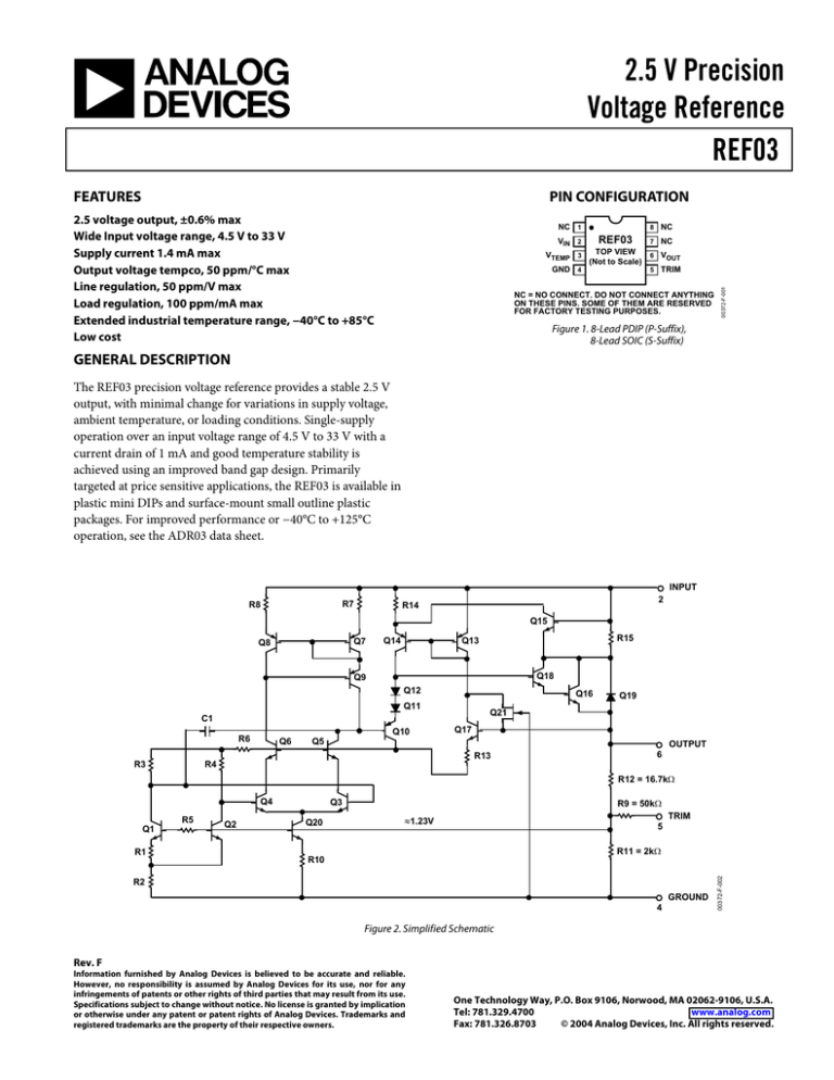
Figure 2. Simplified Schematic
Rev. F
Information furnished by Analog Devices is believed to be accurate and reliable.
However, no responsibility is assumed by Analog Devices for its use, nor for any
infringements of patents or other rights of third parties that may result from its use.
Specifications subject to change without notice. No license is granted by implication
or otherwise under any patent or patent rights of Analog Devices. Trademarks and
registered trademarks are the property of their respective owners.
One Technology Way, P.O. Box 9106, Norwood, MA 02062-9106, U.S.A.
Tel: 781.329.4700
www.analog.com
Fax: 781.326.8703
© 2004 Analog Devices, Inc. All rights reserved.
REF03
TABLE OF CONTENTS
Electrical Specifications ................................................................... 3
Generating a −2.5 V Reference....................................................6
Absolute Maximum Ratings............................................................ 4
Boost Transistor Provides High Output Current......................6
ESD Caution.................................................................................. 4
CMOS DAC Reference .................................................................7
Typical Performance Characteristics ............................................. 5
Outline Dimensions ..........................................................................8
Applications....................................................................................... 6
Ordering Guide .............................................................................8
Generating an Adjustable Bipolar Voltage Reference.............. 6
REVISION HISTORY
6/04—Data Sheet changed from REV. E to REV. F
Updated Formatting......................................................................Universal
Changes to SIMPLIFIED SCHEMATIC........................................................1
Changes to ELECTRICAL SPECIFICATIONS ............................................3
Changes to ORDERING GUIDE....................................................................8
2/04—Data Sheet changed from REV. D to REV. E.
Changes to SIMPLIFIED SCHEMATIC........................................................1
Changes to ELECTRICAL SPECIFICATIONS .............................................2
Changes to ORDERING GUIDE....................................................................3
Replaced TPC 1 ................................................................................................4
8/03—Data Sheet changed from REV. C to REV. D.
Updated format...............................................................................Universal
Change to FEATURES.....................................................................................1
Change to GENERAL DESCRIPTION ..........................................................1
Deleted WAFER TEST LIMITS.......................................................................2
Changes to ELECTRICAL SPECIFICATIONS .............................................2
Changes to ORDERING GUIDE....................................................................3
Added OUTLINE DIMENSIONS ...................................................................7
Revision 0: Initial Version
Rev. F | Page 2 of 8
REF03
ELECTRICAL SPECIFICATIONS
@ VIN = 15 V, −40°C ≤ TA ≤ +85°C, unless otherwise noted.
Table 1.
Parameter
Output Voltage
Output Voltage Tolerance
Output Voltage
Temperature Coefficient1
Line Regulation
Symbol
VO
Min
2.485
TCVO
VIN = 4.5 V to 33 V
Load Regulation
IL = 0 mA to 10 mA
Load Current (Sourcing)
Load Current (Sinking)
Short-Circuit Output Current
Quiescent Supply Current
Turn-On Settling Time2
Output Voltage Noise
Output Adjustment Range
Input Voltage Range
Temperature Voltage Output3
1
Conditions
No Load
No Load
IL
IS
ISC
ISY
tON
en p-p
∆VTRIM
10
−0.3
Output Shorted to Ground
No Load
To ±0.1% of Final Value
0.1 Hz to 10 Hz
RPOT = 10 kΩ
REF03G
Typ
2.500
0.2
Max
2.515
0.6
Unit
V
%
10
20
0.002
60
0.006
50
50
0.005
100
0.010
ppm/°C
ppm/V
%/V
ppm/mA
%/mA
mA
mA
mA
mA
µs
µV p-p
%
V
mV
−0.5
24
1.0
5
6
±11
15
620
±6
4.5
VT
1.4
33
TCVO is measured by the endpoint method, and is equal to
( ) (
)
o
(2.5 × 10 −6 )(125 o C ) in ppm / C
V 85 o C − V − 40 o C
Guaranteed by design.
Limit current in or out of Pin 3 to 50 nA and capacitance on Pin 3 to 30 pF.
+18V
V+
+
10Ω
10µF
2
2
VIN
VIN
VOUT
REF03
REF03
TRIM
GND
5
VOUT
10kΩ
GND
4
+
–18V
6
10µF
4
00372-F-004
3
00372-F-003
2
Figure 4. Output Voltage Trim Method
Figure 3. Burn-In Circuit
Rev. F | Page 3 of 8
REF03
ABSOLUTE MAXIMUM RATINGS
TA = 25°C, unless otherwise noted.
Table 2.
Parameter
Input Voltage
Output Short-Circuit Duration
Operating Temperature Range
REF03G (P, S)
Storage Temperature Range
Junction Temperature Range
Lead Temperature (Soldering, 10 sec)
Rating
40 V
Indefinite
−40°C to +85°C
−65°C to +175°C
−65°C to +175°C
300°C
Absolute maximum ratings apply to both DICE and packaged parts, unless otherwise noted.
Stresses above those listed under Absolute Maximum Ratings may cause permanent damage to the device. This is a stress rating only;
functional operation of the device at these or any other conditions above those indicated in the operational section of this specification is
not implied. Exposure to absolute maximum rating conditions for extended periods may affect device reliability.
Table 3. Package Thermal Resistance
Package Type
8-Lead PDIP (P)
8-Lead SOIC (S)
1
θJA1
110
160
θJC
50
44
Unit
°C/W
°C/W
θJA is specified for worst-case mounting conditions, i.e., θJA is specified for device in socket for PDIP package; θJA is specified for device soldered to printed circuit board
for SOIC package.
ESD CAUTION
ESD (electrostatic discharge) sensitive device. Electrostatic charges as high as 4000 V readily accumulate on
the human body and test equipment and can discharge without detection. Although this product features
proprietary ESD protection circuitry, permanent damage may occur on devices subjected to high energy
electrostatic discharges. Therefore, proper ESD precautions are recommended to avoid performance
degradation or loss of functionality.
Rev. F | Page 4 of 8
REF03
TYPICAL PERFORMANCE CHARACTERISTICS
1.2
20
17
16
15
14
10
15
20
25
30
INPUT VOLTAGE (V)
35
1.1
1.0
0.9
0.8
–40
40
Figure 5. Maximum Load Current vs. Input
Voltage
–20
0
20
40
TEMPERATURE (°C)
60
80
100
00372-F-013
18
00372-F-009
QUIESCENT CURRENT (mA)
19
00372-F-005
MAXIMUM LOAD CURRENT (mA)
TA = 25°C
VIN = 15V
0.1Hz TO 10Hz
VIN = 15V
TA = 25°C
3.2
5.9
OUTPUT VOLTAGE NOISE (µV p-p)
8.6
Figure 13. Typical Distribution of Output
Voltage Noise
Figure 9. Quiescent Current vs. Temperature
65
45
4
8
12
16
20
24
INPUT VOLTAGE (–V)
28
32
72
100
62
320
52
1000
42
3200
–40°C ≤ TA ≤ +85°C
VIN = 15V
10000
32
VIN = 15V
TA = 25°C
22
10
32
Figure 6. Load Regulation (∆IL = 10 mA) vs.
Input Voltage
100
1k
10k
FREQUENCY (Hz)
32000
1M
100k
–45
1.4
VIN = 15V
100
50
12
16
20
INPUT VOLTAGE (V)
24
28
1.2
1.1
1.0
0.9
0.8
0.7
0.6
–40
32
–20
0
20
40
TEMPERATURE (°C)
60
80
100
Figure 11. Normalized Load Regulation
(∆IL = 10 mA) vs. Temperature
Figure 7. Line Regulation vs. Input Voltage
35
VIN = 15V
1000
VIN = 15V
TA = 25°C
30
OUTPUT NOISE (µV p-p)
25
20
15
10
5
10
–20
0
20
40
TEMPERATURE (°C)
60
80
Figure 8. Maximum Load Current vs.
Temperature
100
1
10
00372-F-012
0
–40
100
00372-F-008
MAXIMUM LOAD CURRENT (mA)
00372-F-011
LOAD REG–T/LOAD REG (25°C)
150
00372-F-007
LOAD REGULATION (ppm/V)
1.3
8
45
Figure 14. Typical Distribution of Output
Voltage Tempco
TA = 25°C
4
–30
–15
0
15
30
OUTPUT VOLTAGE TEMPCO (ppm/°C)
Figure 10. Line Regulation vs. Frequency
200
0
00372-F-014
50
10
82
LINE REGULATION (ppm/V)
55
92
00372-F-010
LINE REGULATION (dB)
60
00372-F-006
LOAD REGULATION (ppm/mA)
TA = 25°C
100
1k
10k
FREQUENCY (Hz)
100k
1M
Figure 12. Wideband Output Noise vs.
Bandwidth (0.1 Hz to Frequency Indicated)
Rev. F | Page 5 of 8
REF03
APPLICATIONS
Because an on-board operational amplifier is used to amplify
the basic band gap cell voltage to 2.5 V, supply decoupling is
critical to the transient performance of a voltage reference. The
supply line should be bypassed with a 10 µF tantalum capacitor
in parallel with a 0.01 µF to 0.1 µF ceramic capacitor for best
results, as shown in Figure 15. The bypass capacitors should be
located as close to the reference as possible. Inadequate
bypassing can lead to instabilities.
GENERATING A −2.5 V REFERENCE
Often, there is a requirement for a negative reference voltage.
The simplest method of generating a −2.5 V reference with the
REF03 is to connect an op amp in a gain of −1 to the output, as
shown in Figure 17. This provides both positive and negative
2.5 V references. Figure 18 shows another method of obtaining
a negative reference, in which the current-output element is a
PNP transistor, with the REF03 in a servo loop to ensure that
the output remains 2.5 V below ground.
V+
2
VIN
VOUT
6
REF03
+2.5V
100kΩ
GND
Output bypass capacitors are not generally recommended. If
necessary for high frequency output impedance reduction, the
capacitance value used should be at least 1 µF.
100kΩ
4
2
3
7
OP97
6
–2.5V
00372-F-017
The REF03 provides a stable 2.5 V output voltage with minimal
dependence on load current, line voltage, or temperature. This
voltage is typically used to set an absolute reference point in
data conversion circuits, or in analog circuits such as log amps,
4 to 20 mA transmitters and power supplies. The REF03 is of
particular value in systems requiring a precision reference using
a single 5 V supply rail.
4
V–
V+
10µF
Figure 17. ±2.5 V Reference
+
+5V
0.1µF
2
VIN
1kΩ
REF03
2
VOUT 6
VIN
2.5V
VOUT
00372-F-015
GND
4
6
REF03
Figure 15. Basic Connections
GND
+6.2V
4
–2.5V
2N2905
GENERATING AN ADJUSTABLE BIPOLAR
VOLTAGE REFERENCE
There is often a requirement for an adjustable bipolar reference.
A simple method of generating such a reference is to connect
the output of the REF03 to an op amp in an adjustable gain
configuration, as shown in Figure 16. The trimmable resistor is
then used to generate the desired output voltage from −2.5 V to
+2.5 V.
V+
2
50kΩ
VOUT
6
REF03
50kΩ
50kΩ
2
3
7
+15V
OP97
6
VOUT
–2.5V TO +2.5V
4
Figure 18. −2.5 V Reference
BOOST TRANSISTOR PROVIDES HIGH OUTPUT
CURRENT
When applications require more than 10 mA current delivery,
an external boost transistor may be added to the REF03 to pass
the required current without dissipating excessive power within
the IC. The maximum current output to the system is bounded
only by the capabilities of the boost transistor. Figure 19 shows
this technique, with and without current limiting.
4
GND
V+
Figure 16. Adjustable Bipolar Reference
00372-F-016
VIN
–5V
00372-F-018
2kΩ
Current limiting may be used to prevent damage to the boost
transistor. Figure 19a is an example of no current limit, while
Figure 19b shows the limit that occurs when the voltage
Rev. F | Page 6 of 8
REF03
+5V
dropped across R2 exceeds one VBE (0.6 V). The current limit is
sensitive to the variations of the diodes’ forward drop and the
PNP’s VBE with temperature, and will decrease with increasing
temperature.
REF03
VOUT
V–
GND
6
33Ω
100Ω
19
VREF
4
65Ω
1N4148
R1
40Ω
18
20
VDD RFB
R2
10Ω
OUT
DAC80102
2N2905
2N2905
2
VIN
REF03
REF03
VOUT
GND
4
6
–2.5V
2.49kΩ
A. NO CURRENT LIMIT
VOUT
GND
4
DB11
6
–2.5V
0mA TO 100mA
7
2
3
4
6
VO = 0V TO –2.5V
15
3
–5V
DIGITAL INPUT
OP AMP IS OP43 IF HIGHER AND FASTER SETTING IS REQUIRED,
OP97 IF LOWER SPEED AND HIGHER LINEARITY IS REQUIRED.
2.49kΩ
B. CURRENT LIMITING
AGND
2
DB0 DGND
4
Figure 20. CMOS DAC Reference
00372-F-019
2
VIN
33pF
1
00372-F-020
V+
2
VIN
Figure 19. Output Current Boost
+12V
The REF03 makes an excellent reference for use with CMOS
and bipolar DACs. Figure 20 shows the REF03 connected to the
DAC8012, a 12-bit parallel loading CMOS DAC with memory.
With an OP43 output amplifier for fast settling, the circuit
requires less than 3 mA when driven from TTL gates, and less
than 2 mA when driven from CMOS gates. In situations not
requiring the higher speed of the OP43, enhanced linearity and
some savings in power dissipation can be realized using an
OP97 for the output amplifier. Figure 21 shows a typical
multiplying DAC application using a REF03 reference.
VIN < ±2.5V p-p
VIN
GND
VIN < ±2.5V p-p
VOUT
1/2
DAC80102*
6.9kΩ
+12V
VZ
VIRTUAL ZERO
VIN
REF03
+2.5V
6.9kΩ
1µF
+
VOUT
VOUT = –D/256 × VIN WITH RESPECT TO VIRTUAL ZERO.
*DIGITAL INTERFACE OMITTED FOR CLARITY.
Rev. F | Page 7 of 8
Figure 21. Multiplying CMOS DAC Reference
GND
00372-F-021
VDD
CMOS DAC REFERENCE
REF03
OUTLINE DIMENSIONS
5.00 (0.1968)
4.80 (0.1890)
8
5
4.00 (0.1574)
3.80 (0.1497) 1
4
1.27 (0.0500)
BSC
0.25 (0.0098)
0.10 (0.0040)
0.375 (9.53)
0.365 (9.27)
0.355 (9.02)
6.20 (0.2440)
5.80 (0.2284)
1.75 (0.0688)
1.35 (0.0532)
0.51 (0.0201)
COPLANARITY
SEATING 0.31 (0.0122)
0.10
PLANE
0.50 (0.0196)
× 45°
0.25 (0.0099)
8
5
1
4
0.295 (7.49)
0.285 (7.24)
0.275 (6.98)
0.325 (8.26)
0.310 (7.87)
0.300 (7.62)
0.100 (2.54)
BSC
0.015
(0.38)
MIN
0.180
(4.57)
MAX
8°
0.25 (0.0098) 0° 1.27 (0.0500)
0.40 (0.0157)
0.17 (0.0067)
0.150 (3.81)
0.130 (3.30)
0.110 (2.79)
0.022 (0.56)
0.018 (0.46)
0.014 (0.36)
COMPLIANT TO JEDEC STANDARDS MS-012AA
CONTROLLING DIMENSIONS ARE IN MILLIMETERS; INCH DIMENSIONS
(IN PARENTHESES) ARE ROUNDED-OFF MILLIMETER EQUIVALENTS FOR
REFERENCE ONLY AND ARE NOT APPROPRIATE FOR USE IN DESIGN
Figure 22. 8-Lead Standard Small Outline Package [SOIC]
Narrow Body
(R-8)
S-Suffix
Dimensions shown in millimeters and (inches)
SEATING
PLANE
0.060 (1.52)
0.050 (1.27)
0.045 (1.14)
0.150 (3.81)
0.135 (3.43)
0.120 (3.05)
0.015 (0.38)
0.010 (0.25)
0.008 (0.20)
COMPLIANT TO JEDEC STANDARDS MO-095AA
CONTROLLING DIMENSIONS ARE IN INCHES; MILLIMETER DIMENSIONS
(IN PARENTHESES) ARE ROUNDED-OFF INCH EQUIVALENTS FOR
REFERENCE ONLY AND ARE NOT APPROPRIATE FOR USE IN DESIGN
Figure 23. 8-Lead Plastic Dual In-Line Package [PDIP]
(N-8)
P-Suffix
Dimensions shown in inches and (millimeters)
ORDERING GUIDE
Part Number
REF03GP1
REF03GS2
REF03GS-REEL2
REF03GS-REEL72
REF03GSZ-REEL72, 3
1
2
3
Initial Accuracy
0.2%
0.2%
0.2%
0.2%
0.2%
Temperature Coefficient
10
10
10
10
10
Burn-in is available on commercial and industrial temperature range parts in PDIP package.
For availability and burn-in information on SOIC package, contact your local sales office.
Z = Pb-free part.
© 2004 Analog Devices, Inc. All rights reserved. Trademarks and
registered trademarks are the property of their respective owners.
C00372–0–6/04(F)
Rev. F | Page 8 of 8
Temperature Range
−40°C to +85°C
−40°C to +85°C
−40°C to +85°C
−40°C to +85°C
−40°C to +85°C
Package Option
PDIP
SOIC
SOIC
SOIC
SOIC


