Preliminary Technical Data
FEATURES
PSRR: 100 dB minimum
CMRR: 105 dB typical
Very low supply current: 11 μA maximum
1.8 V to 5 V single-supply or ±0.9 V to ±2.5 V dual-supply
operation
Rail-to-rail input and output
3 mV offset voltage maximum
Very low input bias current: 0.5 pA typical
APPLICATIONS
Pressure and position sensors
Remote security
Medical monitors
Battery-powered consumer equipment
Hazard detectors
11 μA, Rail-to-Rail I/O, Zero Input
Crossover Distortion Amplifiers
ADA4505-1
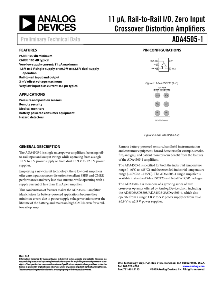
PIN CONFIGURATIONS
Figure 1. 5-Lead SOT23 (RJ-5)
OUT A
V+
V-
NC
+INA
-INA
NC = No Connect
Figure 2. 6-Ball WLCSP (CB-6-2)
GENERAL DESCRIPTION
The ADA4505-1 is single micropower amplifiers featuring railto-rail input and output swings while operating from a single
1.8 V to 5 V power supply or from dual ±0.9 V to ±2.5 V power
supplies.
Employing a new circuit technology, these low cost amplifiers
offer zero input crossover distortion (excellent PSRR and CMRR
performance) and very low bias current, while operating with a
supply current of less than 11 μA per amplifier.
This combination of features makes the ADA4505-1 amplifier
ideal choices for battery-powered applications because they
minimize errors due to power supply voltage variations over the
lifetime of the battery, and maintain high CMRR even for a railto-rail op amp.
Remote battery-powered sensors, handheld instrumentation
and consumer equipment, hazard detectors (for example, smoke,
fire, and gas), and patient monitors can benefit from the features
of the ADA4505-1 amplifiers.
The ADA4505-1is specified for both the industrial temperature
range (−40°C to +85°C) and the extended industrial temperature
range (−40°C to +125°C). The ADA4505-1 single amplifier is
available in standard 5-lead SOT23 and 6-ball WLCSP packages.
The ADA4505-1 is members of a growing series of zero
crossover op amps offered by Analog Devices, Inc., including
the AD8506/AD8508/ADA4505-2/ADA4505-4, which also
operate from a single 1.8 V to 5 V power supply or from dual
±0.9 V to ±2.5 V power supplies.
Rev. PrA
Information furnished by Analog Devices is believed to be accurate and reliable. However, no
responsibility is assumed by Analog Devices for its use, nor for any infringements of patents or other
rights of third parties that may result from its use. Specifications subject to change without notice. No
license is granted by implication or otherwise under any patent or patent rights of Analog Devices.
Trademarks and registered trademarks are the property of their respective owners.
One Technology Way, P.O. Box 9106, Norwood, MA 02062-9106, U.S.A.
Tel: 781.329.4700
www.analog.com
Fax: 781.461.3113
©2009 Analog Devices, Inc. All rights reserved.
ADA4505-1
Preliminary Technical Data
SPECIFICATIONS
ELECTRICAL CHARACTERISTICS—5 V OPERATION
VSY = 5 V, VCM = VSY/2, TA = 25°C, RL = 100 kΩ to GND, unless otherwise specified.
Table 1.
Parameter
INPUT CHARACTERISTICS
Offset Voltage
Input Bias Current
Symbol
Test Conditions/Comments
VOS
0 V ≤ VCM ≤ 5 V
−40°C ≤ TA ≤ +125°C
Min
IB
Typ
Max
Unit
0.5
3
4
2
50
375
1
25
130
5
mV
mV
pA
pA
pA
pA
pA
pA
V
dB
dB
dB
dB
dB
μV/°C
GΩ
pF
pF
0.5
−40°C ≤ TA ≤ +85°C
−40°C ≤ TA ≤ +125°C
Input Offset Current
IOS
Input Voltage Range
Common-Mode Rejection Ratio
CMRR
Large Signal Voltage Gain
AVO
Offset Voltage Drift
Input Resistance
Input Capacitance Differential Mode
Input Capacitance Common Mode
OUTPUT CHARACTERISTICS
Output Voltage High
Output Voltage Low
ΔVOS/ΔT
RIN
CINDM
CINCM
VOH
VOL
Short-Circuit Limit
POWER SUPPLY
Power Supply Rejection Ratio
ISC
Supply Current per Amplifier
ISY
DYNAMIC PERFORMANCE
Slew Rate
Gain Bandwidth Product
Phase Margin
NOISE PERFORMANCE
Voltage Noise
Voltage Noise Density
Current Noise Density
PSRR
0.05
−40°C ≤ TA ≤ +85°C
−40°C ≤ TA ≤ +125°C
−40°C ≤ TA ≤ +125°C
0 V ≤ VCM ≤ 5 V
−40°C ≤ TA ≤ +85°C
−40°C ≤ TA ≤ +125°C
0.05 V ≤ VOUT ≤ 4.95 V
−40°C ≤ TA ≤ +125°C
−40°C ≤ TA ≤ +125°C
0
90
90
85
105
100
105
120
2
220
2.5
4.7
RL = 100 kΩ to GND
−40°C ≤ TA ≤ +125°C
RL = 10 kΩ to GND
−40°C ≤ TA ≤ +125°C
RL = 100 kΩ to VSY
−40°C ≤ TA ≤ +125°C
RL = 10 kΩ to VSY
−40°C ≤ TA ≤ +125°C
VOUT = VSY or GND
4.98
4.98
4.9
4.9
VSY = 1.8 V to 5 V
−40°C ≤ TA ≤ +85°C
−40°C ≤ TA ≤ +125°C
VOUT = VSY/2
−40°C ≤ TA ≤ +125°C
100
100
95
4.99
4.95
2
10
5
5
25
25
±40
110
7
11
15
V
V
V
V
mV
mV
mV
mV
mA
dB
dB
dB
μA
μA
SR
GBP
ΦM
RL = 100 kΩ, CL = 20 pF, G = 1
RL = 1 MΩ, CL = 20 pF, G = 1
RL = 1 MΩ, CL = 20 pF, G = 1
6
50
52
mV/μs
kHz
Degrees
en p-p
en
in
f = 0.1 Hz to 10 Hz
f = 1 kHz
f = 1 kHz
2.95
65
20
μV p-p
nV/√Hz
fA/√Hz
Rev. PrA | Page 2 of 4
Preliminary Technical Data
ADA4505-1
ELECTRICAL CHARACTERISTICS—1.8 V OPERATION
VSY = 1.8 V, VCM = VSY/2, TA = 25°C, RL = 100 kΩ to GND, unless otherwise specified.
Table 2.
Parameter
INPUT CHARACTERISTICS
Offset Voltage
Input Bias Current
Symbol
Test Conditions/Comments
VOS
0 V ≤ VCM ≤ 1.8 V
−40°C ≤ TA ≤ +125°C
Min
IB
Typ
Max
Unit
0.5
3
4
2
50
375
1
25
130
1.8
mV
mV
pA
pA
pA
pA
pA
pA
V
dB
dB
dB
dB
dB
μV/°C
GΩ
pF
pF
0.5
−40°C ≤ TA ≤ +85°C
−40°C ≤ TA ≤ +125°C
Input Offset Current
IOS
Input Voltage Range
Common-Mode Rejection Ratio
CMRR
Large Signal Voltage Gain
AVO
Offset Voltage Drift
Input Resistance
Input Capacitance Differential Mode
Input Capacitance Common Mode
OUTPUT CHARACTERISTICS
Output Voltage High
Output Voltage Low
ΔVOS/ΔT
RIN
CINDM
CINCM
VOH
VOL
Short-Circuit Limit
POWER SUPPLY
Power Supply Rejection Ratio
ISC
Supply Current per Amplifier
ISY
DYNAMIC PERFORMANCE
Slew Rate
Gain Bandwidth Product
Phase Margin
NOISE PERFORMANCE
Voltage Noise
Voltage Noise Density
Current Noise Density
PSRR
0.05
−40°C ≤ TA ≤ +85°C
−40°C ≤ TA ≤ +125°C
−40°C ≤ TA ≤ +125°C
0 V ≤ VCM ≤ 1.8 V
−40°C ≤ TA ≤ +85°C
−40°C ≤ TA ≤ +125°C
0.05 V ≤ VOUT ≤ 1.75 V
−40°C ≤ TA ≤ +125°C
−40°C ≤ TA ≤ +125°C
0
85
85
80
95
95
100
115
2.5
220
2.5
4.7
RL = 100 kΩ to GND
−40°C ≤ TA ≤ +125°C
RL = 10 kΩ to GND
−40°C ≤ TA ≤ +125°C
RL = 100 kΩ to VSY
−40°C ≤ TA ≤ +125°C
RL = 10 kΩ to VSY
−40°C ≤ TA ≤ +125°C
VOUT = VSY or GND
1.78
1.78
1.65
1.65
VSY = 1.8 V to 5 V
−40°C ≤ TA ≤ +85°C
−40°C ≤ TA ≤ +125°C
VOUT = VSY/2
−40°C ≤ TA ≤ +125°C
100
100
95
1.79
1.75
2
12
5
5
25
25
±3.8
110
7
11
15
V
V
V
V
mV
mV
mV
mV
mA
dB
dB
dB
μA
μA
SR
GBP
ΦM
RL = 100 kΩ, CL = 20 pF, G = 1
RL = 1 MΩ, CL = 20 pF, G = 1
RL = 1 MΩ, CL = 20 pF, G = 1
6.5
50
52
mV/μs
kHz
Degrees
en p-p
en
in
f = 0.1 Hz to 10 Hz
f = 1 kHz
f = 1 kHz
2.95
65
20
μV p-p
nV/√Hz
fA/√Hz
Rev. PrA | Page 3 of 4
ADA4505-1
Preliminary Technical Data
ABSOLUTE MAXIMUM RATINGS
THERMAL RESISTANCE
Table 3.
Parameter
Supply Voltage
Input Voltage
Input Current1
Differential Input Voltage2
Output Short-Circuit Duration to GND
Storage Temperature Range
Operating Temperature Range
Junction Temperature Range
Lead Temperature (Soldering, 60 sec)
θJA is specified for the worst-case conditions, that is, a device
soldered in a circuit board for surface-mount packages. This
was measured using a standard 2-layer board, unless otherwise
specified.
Rating
5.5 V
±VSY ± 0.1 V
±10 mA
±VSY
Indefinite
−65°C to +150°C
−40°C to +125°C
−65°C to +150°C
300°C
Table 4. Thermal Resistance
Package Type
5-Lead SOT23 (RJ-5)
6-Ball WLCSP (CB-6-2)
2-Layer PCB (1SOP)
4-Layer PCB (2SOP)
1
Input pins have clamp diodes to the supply pins. Input current should be
limited to 10 mA or less whenever the input signal exceeds the power
supply rail by 0.5 V.
2
Differential input voltage is limited to 5 V or the supply voltage, whichever
is less.
Stresses above those listed under Absolute Maximum Ratings
may cause permanent damage to the device. This is a stress
rating only; functional operation of the device at these or any
other conditions above those indicated in the operational
section of this specification is not implied. Exposure to absolute
maximum rating conditions for extended periods may affect
device reliability.
1
Junction-to-board thermal resistance.
ESD CAUTION
©2009 Analog Devices, Inc. All rights reserved. Trademarks and
registered trademarks are the property of their respective owners.
PR08288-0-5/09(PrA)
Rev. PrA | Page 4 of 4
θJA
TBD
θJB1
TBD
θJC
TBD
Unit
°C/W
TBD
TBD
TBD
TBD
N/A
N/A
°C/W
°C/W


