User Guide 049
ISL8117AEVAL1Z Evaluation Board User Guide
Description
Key Features
The ISL8117AEVAL1Z evaluation board (shown in Figure 4 on
page 4) features the ISL8117A. The ISL8117A is a 60V high
voltage synchronous buck controller that offers external
soft-start, independent enable functions and integrates
UV/OV/OC/OT protection. Its current mode control architecture
and internal compensation network keep peripheral
component count minimal. Programmable switching
frequency ranging from 100kHz to 2MHz helps to optimize
inductor size while the strong gate driver delivers up to 30A for
the buck output.
• Wide input range: 18V to 60V
• High light-load efficiency in pulse skipping DEM operation
• Programmable soft-start
• Optional DEM/CCM operation
• Supports prebias output with SR soft-start
• External frequency sync
• PGOOD indicator
• OCP, OVP, OTP, UVP protection
Specifications
• Back biased from output to improve efficiency
The ISL8117AEVAL1Z evaluation board is designed for high
current applications. The current rating of the
ISL8117AEVAL1Z is limited by the FETs and inductor selected.
The ISL8117A gate driver is capable of delivering up to 20A for
the buck output as long as the proper FETs and inductor are
provided. The electrical ratings of the ISL8117AEVAL1Z are
shown in Table 1.
References
ISL8117A Datasheet
Ordering Information
PART NUMBER
TABLE 1. ELECTRICAL RATING
PARAMETER
Input Voltage
ISL8117AEVAL1Z
DESCRIPTION
High voltage PWM step-down
synchronous buck controller evaluation
board
RATING
18V to 60V
Switching Frequency 300kHz
Output Voltage
12V
Output Current
20A
OCP Set Point
Minimum 25A at ambient room temperature
VIN
VOUT
UGATE
LGATE/OCS
ISL8117A
EXTBIAS
EN
ISL80138
MOD/SYNC VCC5C
DEM
DISABLE
CCM
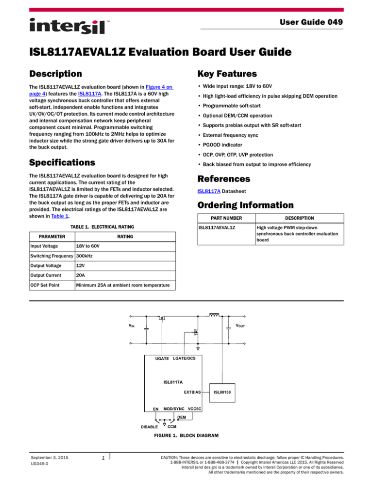
FIGURE 1. BLOCK DIAGRAM
September 3, 2015
UG049.0
1
CAUTION: These devices are sensitive to electrostatic discharge; follow proper IC Handling Procedures.
1-888-INTERSIL or 1-888-468-3774 | Copyright Intersil Americas LLC 2015. All Rights Reserved
Intersil (and design) is a trademark owned by Intersil Corporation or one of its subsidiaries.
All other trademarks mentioned are the property of their respective owners.
User Guide 049
Recommended Testing
Equipment
The following materials are recommended to perform testing:
• 0V to 60V power supply with at least 30A source current
capability
• Electronic loads capable of sinking current up to 30A
• Digital Multimeters (DMMs)
• 100MHz quad-trace oscilloscope
Quick Test Guide
1. Jumper J5 provides the option to select CCM or DEM. Please
refer to Table 2 for the desired operating option. Ensure that
the circuit is correctly connected to the supply and electronic
loads prior to applying any power. Please refer to Figure 3 for
proper set-up.
2. Turn on the power supply.
3. Adjust input voltage VIN within the specified range and
observe output voltage. The output voltage variation should
be within 3%.
4. Adjust load current within the specified range and observe
output voltage. The output voltage variation should be
within 3%.
5. Use an oscilloscope to observe output voltage ripple and
Phase node ringing. For accurate measurement, please refer
to Figure 2 for proper test set-up.
TABLE 2. DESIRED OPERATING OPTIONS
JUMPER
#
J5
J6
POSITION
FUNCTION
CCM (Pin 1-2)
Continuous current mode
DEM (Pin 2-3)
Diode emulation mode
(Pin 1-2)
Disable the PWM
OUTPUT CAP
OR MOSFET
FIGURE 2. PROPER PROBE SET-UP TO MEASURE OUTPUT RIPPLE
AND PHASE NODE RINGING
Functional Description
The ISL8117AEVAL1Z is the same test board used by the Intersil
application engineers and IC designers to evaluate the
performance of the ISL8117A QFN IC. The board is set to provide
an easy and complete evaluation of all the IC and board
functions.
As shown in Figure 3 on page 3, 18V to 60V VIN is supplied to J1
(+) and J2 (-). The regulated 12V output on J3 (+) and J4 (-) can
supply up to 20A to the load. Due to the high thermal efficiency,
the evaluation board can run at 20A continuously without airflow
under room temperature ambient conditions.
Test points TP1 through TP19 provide easy access to IC pin and
external signal injection terminals.
As shown in Table 2, connector J5 provides selection of either
CCM mode (shorting pin 1 and pin 2) or DEM mode (shorting
pin 2 and pin 3). Connector J6 provides an option to disable the
converter by shorting its pin 1 and 2.
Operating Range
The input voltage range is from 18V to 60V for an output voltage
of 12V. If the output voltage is set to a lower value, the minimum
VIN can be reset to a lower value by changing the ratio of R4 and
R5. The minimum EN threshold that VIN can be set to is 4.5V.
The rated load current is 20A with the OCP point set at minimum
25A at room ambient condition.
The operating temperature range is from -40°C to +125°C.
Please note that airflow is needed for higher temperature
ambient conditions.
PCB Layout Guideline
Careful attention to layout requirements is necessary for
successful implementation of an ISL8117A based DC/DC
converter. The ISL8117A switches at a very high frequency and
therefore the switching times are very short. At these switching
frequencies, even the shortest trace has significant impedance.
Also, the peak gate drive current rises significantly in an
extremely short time. Transition speed of the current from one
device to another causes voltage spikes across the
interconnecting impedances and parasitic circuit elements.
These voltage spikes can degrade efficiency, generate EMI, and
increase device overvoltage stress and ringing. Careful
component selection and proper PC board layout minimizes the
magnitude of these voltage spikes.
There are three sets of critical components in a DC/DC converter
using the ISL8117A:
• The controller
• The switching power components
• The small signal components
The switching power components are the most critical from a
layout point of view because they switch a large amount of
energy, which tends to generate a large amount of noise. The
critical small signal components are those connected to sensitive
nodes or those supplying critical bias currents. A multilayer
printed circuit board is recommended.
Submit Document Feedback
2
UG049.0
September 3, 2015
User Guide 049
Layout Considerations
1. The input capacitors, upper FET, lower FET, inductor and
output capacitor should be placed first. Isolate these power
components on the top side of the board with their ground
terminals adjacent to one another. Place the input high
frequency decoupling ceramic capacitors very close to the
MOSFETs.
2. Use separate ground planes for power ground and small
signal ground. Connect the SGND and PGND together close to
the IC. DO NOT connect them together anywhere else.
3. The loop formed by the input capacitor, the top FET and the
bottom FET must be kept as small as possible.
4. Ensure the current paths from the input capacitor to the
MOSFET, to the output inductor and the output capacitor are
as short as possible with maximum allowable trace widths.
5. Place the PWM controller IC close to the lower FET. The LGATE
connection should be short and wide. The IC can be best
placed over a quiet ground area. Avoid switching ground loop
currents in this area.
6. Place VCC5V bypass capacitor very close to the VCC5V pin of
the IC and connect its ground to the PGND plane.
7. Place the gate drive components (optional BOOT diode and
BOOT capacitors) together near the controller IC.
8. The output capacitors should be placed as close to the load as
possible. Use short wide copper regions to connect output
capacitors to load in order to avoid inductance and
resistances.
9. Use copper filled polygons or wide but short trace to connect
the junction of the upper FET, lower FET and output inductor.
Also keep the PHASE node connection to the IC short. DO NOT
unnecessarily oversize the copper islands for the PHASE
node. Since the phase nodes are subjected to very high dv/dt
voltages, the stray capacitor formed between these islands
and the surrounding circuitry will tend to couple switching
noise.
10. Route all high speed switching nodes away from the control
circuitry.
11. Create a separate small analog ground plane near the IC.
Connect the SGND pin to this plane. All small signal grounding
paths including feedback resistors, current limit setting
resistor, soft-starting capacitor and EN pull-down resistors
should be connected to this SGND plane.
12. Separate the current sensing trace from the PHASE node
connection.
13. Ensure the feedback connection to the output capacitor is
short and direct.
A
+
+
LOAD
-
+
V
VIN
+
-
-
A
-
FIGURE 3. PROPER TEST SET-UP
Submit Document Feedback
3
UG049.0
September 3, 2015
User Guide 049
FIGURE 4. ISL8117AEVAL1Z TOP SIDE
FIGURE 5. ISL8117AEVAL1Z BOTTOM SIDE
.
Submit Document Feedback
4
UG049.0
September 3, 2015
User Guide 049
Typical Evaluation Board Performance Curves
100
100
95
95
90
VIN = 48V
85
VIN = 60V
VIN = 36V
80
VIN = 24V
EFFICIENCY (%)
EFFICIENCY (%)
90
VIN = 18V
75
VIN = 60V
65
4
6
8
10
12
IOUT (A)
14
16
18
60
20
0
FIGURE 6. CCM EFFICIENCY vs LOAD
2
4
6
8
10
12
IOUT (A)
14
16
18
20
12.20
12.18
12.18
VIN = 18V
12.16
12.14
IO = 0A
12.16
12.14
VIN = 48V
12.12
VOUT (V)
VOUT (V)
VIN = 18V
FIGURE 7. DEM EFFICIENCY vs LOAD
12.20
12.10
12.08
12.12
12.10
12.08
12.06
12.06
VIN = 60V
12.04
12.02
12.00
VIN = 24V
75
65
2
VIN = 36V
80
70
0
VIN = 48V
85
70
60
VIN = 48V, unless otherwise noted.
12.04
VIN = 36V
0
2
4
6
8
10
VIN = 24V
12
14
16
18
20
IOUT (A)
FIGURE 8.
IO = 20A
IO = 10A
12.02
12.00
18
23
28
33
38
43
48
53
58
VIN (V)
FIGURE 9. CCM MODE LINE REGULATION
CCM MODE LOAD REGULATION
5
PHASE 50V/DIV
CCM
IIN (A)
0.5
LGATE 5V/DIV
0.05
IL 10A/DIV
DEM
0.005
0.01
0.1
1
10
IOUT (A)
FIGURE 10. INPUT CURRENT COMPARISON WITH MODE = CCM/DEM
Submit Document Feedback
5
2µs/DIV
FIGURE 11. PHASE, LGATE AND INDUCTOR CURRENT WAVEFORMS
UG049.0
September 3, 2015
User Guide 049
Typical Evaluation Board Performance Curves
VOUT 50mV/DIV
NO LOAD VIN = 48V
20A LOAD VIN = 48V
VIN = 48V, unless otherwise noted. (Continued)
NO LOAD VIN = 48V
VOUT 50mV/DIV
20A LOAD VIN = 48V
VOUT 50mV/DIV
VOUT 50mV/DIV
4µs/DIV
1ms/DIV
FIGURE 12. OUTPUT RIPPLE, MODE = CCM
FIGURE 13. OUTPUT RIPPLE, MODE = DEM
VOUT 5V/DIV
VOUT 5V/DIV
PHASE 50V/DIV
PHASE 50V/DIV
LGATE 5V/DIV
LGATE 5V/DIV
IL 10A/DIV
IL 10A/DIV
4ms/DIV
4ms/DIV
FIGURE 14. START-UP WAVEFORMS; MODE = CCM, LOAD = 0A,
VIN = 48V
VOUT 5V/DIV
VOUT 5V/DIV
SS 2V/DIV
SS 2V/DIV
EN 5V/DIV
EN 5V/DIV
PGOOD 5V/DIV
PGOOD 5V/DIV
20ms/DIV
FIGURE 16. START-UP WAVEFORMS; MODE = CCM, LOAD = 0A,
VIN = 48V
Submit Document Feedback
6
FIGURE 15. START-UP WAVEFORMS; MODE = DEM, LOAD = 0A,
VIN = 48V
20ms/DIV
FIGURE 17. START-UP WAVEFORMS; MODE = DEM, LOAD = 0A,
VIN = 48V
UG049.0
September 3, 2015
User Guide 049
Typical Evaluation Board Performance Curves
VIN = 48V, unless otherwise noted. (Continued)
SYNC 5V/DIV
SS 500mV/DIV
LGATE 5V/DIV
vOUT 10V/DIV
IL 10A/DIV
PGOOD 5V/DIV
2µs/DIV
4ms/DIV
FIGURE 18. TRACKING; VIN = 48V, LOAD = 0A, MODE = CCM
FIGURE 19. FREQUENCY SYNCHRONIZATION; VIN = 48V, LOAD = 0A,
DEFAULT fSW = 300kHz, SYNC fSW = 330kHz
vOUT 10V/DIV
vOUT 200mV/DIV
SS 5V/DIV
PGOOD 5V/DIV
IL 20A/DIV
IOUT 10A/DIV
400µs/DIV
FIGURE 20. LOAD TRANSIENT RESPONSE; VIN = 48V, 0A TO 20A
1A/µs STEP LOAD, CCM MODE
Submit Document Feedback
7
200ms/DIV
FIGURE 21. OCP RESPONSE, OUTPUT SHORT CIRCUITED TO
GROUND AND RELEASED, CCM MODE, VIN = 48V
NO LOAD TO SHORT AND RELEASE
UG049.0
September 3, 2015
4.7u/100V
4.7u/100V
4.7u/100V
SPST
J6
1
R4
R5
0.1u/25V
C5
C23
C17
C15
C18
C30
C31
C13
C16
C12
J2
R9 20
4
3
2
1
R23 0
IN
OUT
14
exbi
vcc5
D1
GND
1A/100V
en
R20
R27 0
R19
boot
13
14
15
VIN
BOOT
Q1
NMOS
MOD/SYNC
2
UG
PGOOD
12
R12 0
SS/TRK
VCC5V
10
isen
FB
9
3.3u/30A
C22
C10
C9 C8
C11
R15
20
vcc5
10u/10V
Q3
NMOS
Q4
NMOS
J4
R16
6
5
4
3
2
1
TP3
0
1
R8
DNP
lg
C6
220p/50V
R17 0
R3
16.5k
R28
43.2k
10u/50V
VOUT
10u/50V
10u/50V
330u/35V
1u/50V
C1
comp
C42
100p/50V
R18
10
GND
CON1
10u/50V 10u/50V
10u/50V 10u/50V 10u/50V
vout
R1
43.2k
C36
C37 C40 C38 C32
fb
TRACKING
R26
CON1
L1
C7
DNP
C41
1n/50V
VCC5
DNP
ph
8
C3
0.047u/25V
6
5
ss
TP19
CON1
LGATE/OCS
4
SYNC
PGND
R6
0
ISEN
COMP
JMP
11
6
5
4
3
2
1
vout
R7 3.3k
RT
J3
ug
ISL8117A
3
rt
DNP
1
PHASE
R22
TP2
1
R13 0
pg
3
2
1
C2
1u/25V
R11 0
R14 100k
J5
Q2
NMOS
DNP
R2
2.26k
10u/50V
10u/50V
10u/50V 10u/50V
C33 C35 C39 C34
1
comp
1
mod
1
isen
1
vcc5
1
fb
1
lg
1
ph
1
ug
1
boot
1
exbi
1
vin
1
en
1
ss
1
pg
1
1
rt
UG049.0
September 3, 2015
Title
<Title>
TP18
CON1
TP4
TP5
TP6
TP7
TP8
TP9
TP10 TP11 TP12 TP13 TP14 TP15 TP1
TP16 TP17
CON1 CON1 CON1 CON1 CON1 CON1 CON1 CON1 CON1 CON1 CON1 CON1 CON1 CON1 CON1
Size
A
Date:
FIGURE 22. ISL8117AEVAL1Z SCHEMATIC
ISL8117AEVAL1Z Rev A
Vin:18V~60V
Vout:12V 20A 300K
Document Number
<Doc>
Tuesday December 09 2014
Rev
<Rev
Sheet
1
of
1
User Guide 049
1
mod
U2
EXTBIAS
10k
ISL80138
16
R21
15
8
0.1u/25V
12
EN
C20
10k
ADJ
17
EN
SGND
7
GND
30.9k
en
R25
100u/100V VIN
100u/100V
vin
7
8
2
4.7u/100V
4.7u/100V
4.7u/100V
4.7u/100V
4.7u/100V 4.7u/100V
C24
C4
0.1u/100V
10k
0.1u/100V
C21
U3
R24 0
C26
C14
90.9k
vout
C25
J1
4
3
2
1
4.7u/100V
10u/10V
2
Submit Document Feedback
Schematic
User Guide 049
Bill of Materials
MANUFACTURER
PART
REFERENCE
DESIGNATOR
QTY UNITS
ISL8117AEVAL1ZREVAPCB
1
ea.
ECJ-1VC1H101J
1
ea.
06035C102KAT2A
1
C0603X7R101-104KNE
DESCRIPTION
MANUFACTURER
PWB-PCB, ISL8117EVAL1Z, REVA, ROHS
SHENZHEN MULTILAYER PCB
TECHNOLOGY CO.,LTD
C42
CAP, SMD, 0603, 100pF, 50V, 5%, C0G, ROHS
PANASONIC
ea.
C41
CAP, SMD, 0603, 1000pF, 50V, 10%, X7R, ROHS
AVX
2
ea.
C4, C21
CAP, SMD, 0603, 0.1µF, 100V, 10%, X7R, ROHS
VENKEL
GRM39X7R104K025AD
2
ea.
C5, C20
CAP, SMD, 0603, 0.1µF, 25V, 10%, X7R, ROHS
MURATA
C1608X5R1H105K
2
ea.
C2, C22
CAP, SMD, 0603, 1µF, 50V, 10%, X5R, ROHS
TDK
ECJ-1VB1A106M
2
ea.
C1, C17
CAP, SMD, 0603, 10µF, 10V, 20%, X5R, ROHS
PANASONIC
GRM188R71H221KA01D
1
ea.
C6
CAP, SMD, 0603, 220pF, 50V, 10%, X7R, ROHS
MURATA
GRM188R71E473KA01D
1
ea.
C3
CAP, SMD, 0603, 0.047µF, 25V, 10%, X7R, ROHS MURATA
0
ea.
C7
CAP, SMD, 0603, DNP-PLACE HOLDER, ROHS
UMK325BJ106KM-T
12
ea.
a) C8, C9, C10, C32,
C33, C34, C35, C36,
C37
CAP, SMD, 1210, 10µF, 50V, 10%, X5R, ROHS
TAIYO YUDEN
UMK325BJ106KM-T
0
ea.
b) C38, C39, C40.
CAP, SMD, 1210, 10µF, 50V, 10%, X5R, ROHS
TAIYO YUDEN
CGA6M3X7S2A475K200AB
10
ea.
a) C12, C13, C14, C15, CAP, SMD, 1210, 4.7µF, 100V, 10%, X7S, ROHS
C23, C24, C25, C26
TDK
CGA6M3X7S2A475K200AB
0
ea.
b) C30, C31
CAP, SMD, 1210, 4.7µF, 100V, 10%, X7S, ROHS
TDK
EEE-FP1V331AP
1
ea.
C11
CAP, SMD, 10x10.2mm, 330µF, 35V, 20%,
ALUM.ELEC., ROHS
PANASONIC
EMVH101GDA101MLH0S
2
ea.
C16, C18
CAP, SMD, 16x16.5mm, 100µF, 100V, 20%,
ALUM.ELEC., ROHS
UNITED CHEMI-CON
IHLP6767GZER3R3M11
1
ea.
L1
COIL-PWR INDUCTOR, SMD, 17.15mmSQ., 3.3µH, VISHAY
20%, 35A, ROHS
5007
19
ea.
TP1-TP19
CONN-COMPACT TEST PT, VERTICAL, WHT, ROHS
68000-236HLF
1
ea.
J5
CONN-HEADER, 1x3, BREAKAWY 1X36, 2.54mm, BERG/FCI
ROHS
69190-202HLF
1
ea.
J6
CONN-HEADER, 1X2, RETENTIVE, 2.54mm,
0.230X 0.120, ROHS
BERG/FCI
SPC02SYAN
2
ea.
J5, J6
CONN-JUMPER, SHORTING, 2PIN, BLACK, GOLD,
ROHS
SULLINS
MBR1H100SFT3G
1
ea.
D1
DIODE-RECTIFIER, SMD, 2P, S0D-123FL, 100V, 1A, ON SEMICONDUCTOR
ROHS
ISL80138IVEAJZ
1
ea.
U3
IC-40V LDO ADJ. LINEAR REGULATOR, 14P,
HTSSOP, ROHS
ISL8117AFRZ
1
ea.
U2
IC-55V SWITCHING CONTROLLER, 16P, QFN, ROHS INTERSIL
BSC067N06LS3G
4
ea.
Q1, Q2, Q3, Q4
TRANSISTOR-MOS, N-CHANNEL, 8P, PG-TDSON-8, INFINEON TECHNOLOGY
60V, 50A, ROHS
RK73H1JT10R0F
1
ea.
R18
RES, SMD, 0603, 10Ω, 1/10W, 1%, TF, ROHS
KOA
ERJ-3EKF20R0V
2
ea.
R9, R15
RES, SMD, 0603, 20Ω, 1/10W, 1%, TF, ROHS
PANASONIC
CR0603-10W-000T
9
ea.
R6, R11, R12, R13,
R16, R17, R23, R24,
R27
RES, SMD, 0603, 0Ω, 1/10W, TF, ROHS
VENKEL
RK73H1JT1002F
3
ea.
R5, R19, R21
RES, SMD, 0603, 10k, 1/10W, 1%, TF, ROHS
KOA
Submit Document Feedback
9
KEYSTONE
INTERSIL
UG049.0
September 3, 2015
User Guide 049
Bill of Materials
MANUFACTURER
PART
CR0603-10W-1003FT
REFERENCE
DESIGNATOR
QTY UNITS
DESCRIPTION
MANUFACTURER
1
ea.
R14
RES, SMD, 0603, 100k, 1/10W, 1%, TF, ROHS
VENKEL
1
ea.
R3
RES, SMD, 0603, 8.2k, 1/10W, 1%, TF, ROHS
RC0603FR-072K26L
1
ea.
R2
RES, SMD, 0603, 2.26k, 1/10W, 1%, TF, ROHS
YAGEO
RC0603FR-0730K9L
1
ea.
R20
RES, SMD, 0603, 30.9k, 1/10W, 1%, TF, ROHS
YAGEO
MCR03EZPFX3301
1
ea.
R7
RES, SMD, 0603, 3.3kΩ, 1/10W, 1%, TF, ROHS
ROHM
RC0603FR-0743K2L(PbFREE)
2
ea.
R1, R28
RES, SMD, 0603, 43.2k, 1/10W, 1%, TF, ROHS
YAGEO
ERJ-3EKF9092V
1
ea.
R4
RES, SMD, 0603, 90.9k, 1/10W, 1%, TF, ROHS
PANASONIC
0
ea.
R22, R25, R26
RES, SMD, 0603, DNP-PLACE HOLDER, ROHS
0
ea.
R8
RES, SMD, 1206, DNP, DNP, DNP, TF, ROHS
7795
2
ea.
J1, J2
HDWARE, TERMINAL, M4 METRIC SCREW, TH, 4P, KEYSTONE
SNAP-FIT, ROHS
7798
2
ea.
J3, J4
HDWARE, TERMINAL, M4 METRIC SCREW, TH, 6P, KEYSTONE
SNAP-FIT, ROHS
R25-1001002
4
ea.
Four corners
STANDOFF, M2.5, 10mm, METRIC, F/F, HEX,
THREADED, ROHS
HARWIN INC
29301
4
ea.
Four corners
SCREW, M2.5, 6mm, METRIC, PANHEAD,
SLOTTED, STEEL, ROHS
KEYSTONE
ISL8117AEVAL1Z PCB Layout
FIGURE 23. SILKSCREEN TOP
Submit Document Feedback
10
FIGURE 24. TOP LAYER
UG049.0
September 3, 2015
User Guide 049
ISL8117AEVAL1Z PCB Layout (Continued)
FIGURE 25. SECOND LAYER (SOLID GROUND)
FIGURE 26. THIRD LAYER
FIGURE 27. BOTTOM LAYER
FIGURE 28. SILKSCREEN BOTTOM
Intersil Corporation reserves the right to make changes in circuit design, software and/or specifications at any time without notice. Accordingly, the reader is
cautioned to verify that the document is current before proceeding.
For information regarding Intersil Corporation and its products, see www.intersil.com
Submit Document Feedback
11
UG049.0
September 3, 2015
