VOL. 10, NO 14, AUGUST 2015
ISSN 1819-6608
ARPN Journal of Engineering and Applied Sciences
©2006-2015 Asian Research Publishing Network (ARPN). All rights reserved.
www.arpnjournals.com
L Z SOURCE INVERTER WITH CLOSED LOOP CONTROL SYSTEM
Chokkalingam C. and M. Pushpavalli
Department of Electrical and Electronics Engineering, Sathyabama University, Chennai, India
E-Mail: clingam@gmail.com
ABSTRACT
This paper proposes closed loop of LZ source inverter. This inverter has three diode and two inductors in the main
circuit. It boosts up the input DC voltage. The traditional inverters have capacitors in the main circuit which lead to many
problems such as resonance produced in the circuit, voltage surge which can damage the devices, large volume, more cost,
and reduced life span of the system. This inverter does not have capacitor in the main circuit and therefore eliminates the
problems present in traditional inverters. But in industrial applications the control of output voltage becomes a difficult
factor. The sudden voltage change creates many problems such as instability in the system, damage to devices etc. The
voltage control is an important factor for stable operation of the system in real time. It can be achieved using the closed
loop control of L Z source inverter.
Keywords: voltage, PI controller, LZ inverter, load change.
1. INTRODUCTION
In the open loop system the voltage in the system
change at different levels due to variation in the load. This
can lead to many problems such as damage of components
in the system and interruption in the operation of the
system. The cost of the system is also high due to high cost
of devices. It again decreases the efficiency of the whole
system. So it becomes a necessity to maintain the voltage
in the system. In industrial applications the stability and
reliability of the system is very important. These problems
are overcome using the closed loop control. The closed
loop system maintains the voltage at constant level which
improves the system reliably and protects the device from
sudden voltage changes produced in the system due to load
variations. This paper shows the problems that are existing
with open loop and how it is overcome using the closed
loop control.
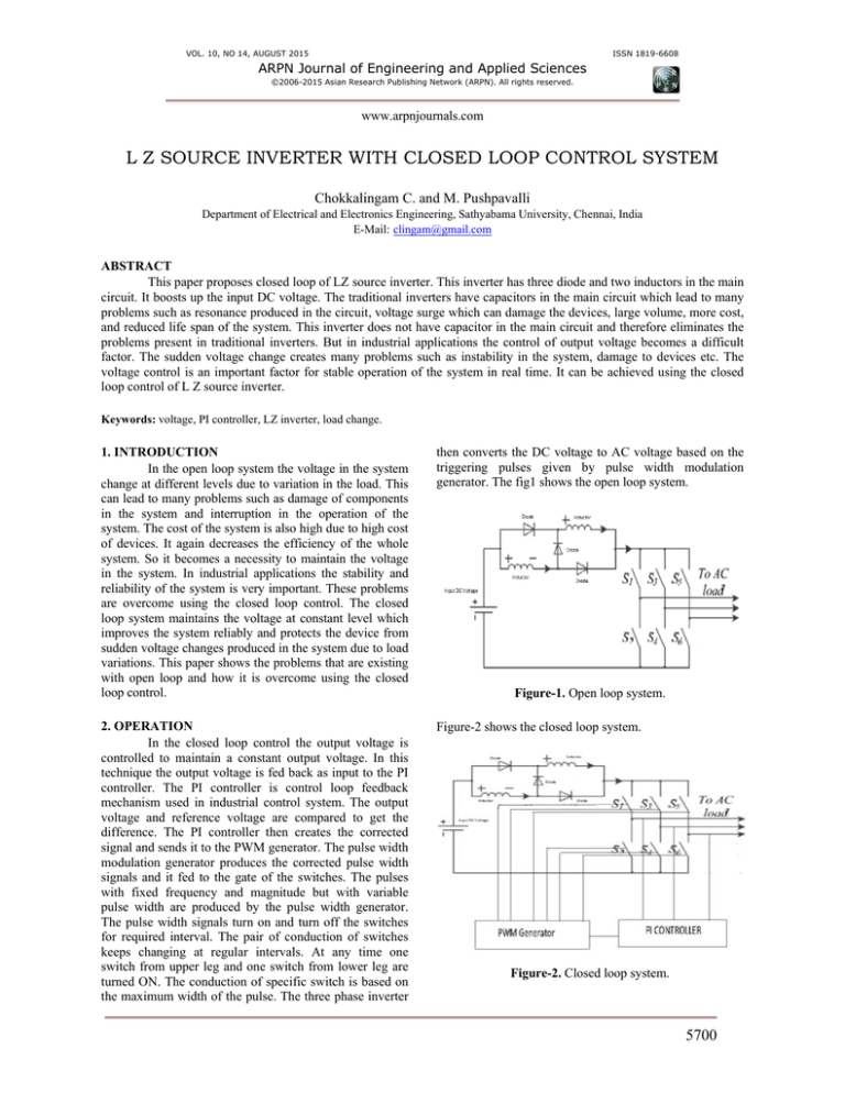
then converts the DC voltage to AC voltage based on the
triggering pulses given by pulse width modulation
generator. The fig1 shows the open loop system.
2. OPERATION
In the closed loop control the output voltage is
controlled to maintain a constant output voltage. In this
technique the output voltage is fed back as input to the PI
controller. The PI controller is control loop feedback
mechanism used in industrial control system. The output
voltage and reference voltage are compared to get the
difference. The PI controller then creates the corrected
signal and sends it to the PWM generator. The pulse width
modulation generator produces the corrected pulse width
signals and it fed to the gate of the switches. The pulses
with fixed frequency and magnitude but with variable
pulse width are produced by the pulse width generator.
The pulse width signals turn on and turn off the switches
for required interval. The pair of conduction of switches
keeps changing at regular intervals. At any time one
switch from upper leg and one switch from lower leg are
turned ON. The conduction of specific switch is based on
the maximum width of the pulse. The three phase inverter
Figure-2 shows the closed loop system.
Figure-1. Open loop system.
Figure-2. Closed loop system.
5700
VOL. 10, NO 14, AUGUST 2015
ISSN 1819-6608
ARPN Journal of Engineering and Applied Sciences
©2006-2015 Asian Research Publishing Network (ARPN). All rights reserved.
www.arpnjournals.com
3. BLOCK DIAGRAM
The input DC voltage is applied to main circuit.
The main circuit produces the amplified DC voltage at the
output. The amplified DC voltage is then fed as input to
the three phase inverter. The switches in the three phase
inverter are triggered by the pulses that are generator by
the PWM generator. The three phase inverter converts the
DC voltage to the output AC voltage. The output AC
voltage is then fed as input to the load. The block diagram
of open loop system is shown in Figure-3.
Figure-5. Non Shoot through mode.
Mode 2: Shoot through state
In this mode the diodes in the upper and lower
arm are conducting and the diode in the middle arm circuit
is in off state. The three phase inverter side is shorted by
the upper and lower switching devices. So the inductors in
the upper and lower arm are connected in parallel and
inductors stores energy in this mode. The circuit diagram
is shown in Figure-6.
Figure-3. Existing system block diagram.
Similar to the open loop system the input DC
voltage is amplified using the main circuit and three phase
inverter converters the DC voltage to AC voltage.
Additionally, the output voltage is fed back to PI
controller where it is compared with the reference signal to
produce the error signal if there are any differences. The
obtained signal is sent to PWM generator which then
creates pulse width of required width and triggers the
switches present in the three phase inverter such that the
output voltage is maintained at constant level. The block
diagram of closed loop control system is shown in Figure4.
Figure-6. Shoot through mode.
5. SIMULATION RESULTS OF EXISTING OPEN
LOOP SYSTEM
The simulation of existing and proposed system
has been carried out using the MATLAB simulink tool.
The simulation of the existing system shows the problems
present in the existing system. The simulation diagram is
shown in Figure-7.
Figure-4. Proposed closed loop diagram.
4. OPERATION MODES
The operating modes of the system are explained
below.
Mode 1: Non-Shoot through state
In this mode the diodes in the upper and lower
arm are in off state and the diode in the middle arm of the
circuit is conducting. So the inductors in the upper and
lower arm are connected in series. In this state the
inductors transfer the energy from the input source to the
output load. The circuit diagram is shown in Figure-5.
Figure-7. Existing open loop system.
The simulation results of existing system are
shown below. When the input DC voltage is 48 V and the
5701
VOL. 10, NO 14, AUGUST 2015
ISSN 1819-6608
ARPN Journal of Engineering and Applied Sciences
©2006-2015 Asian Research Publishing Network (ARPN). All rights reserved.
www.arpnjournals.com
output resistive load is 100 ohm. It is found that output
voltage at the load is 180V. The output voltage waveform
is shown in Figure-8.
Figure-10. Proposed closed loop system.
The simulation result of the closed loop system is
shown below. When the input DC voltage is 48 V and the
output resistive load is 100 ohm. The output voltage at the
load is 100V. The output voltage is shown in Figure-11.
Figure-8. Output voltage at input voltage 48V and load
resistance 100ohm.
When the input DC voltage is 48V and the load is
changed to 50ohm from 100 ohm. It is found that the
output voltage at the load is 120V. The output voltage is
shown in Figure-9.
Figure-11. Output voltage waveform at input voltage 48V
and load resistance 100ohm.
Figure-9. Output voltage at input voltage 48V and load
resistance 50ohm.
When the input DC voltage is 48V the load is
changed to 50ohm from 100 ohm. The output voltage at the
load is maintained at 100V. The output voltage is shown in
Figure-12.
6. SIMULATION RESULTS OF MODIFIED CLOSED
LOOP SYSTEM
The simulation of existing and proposed system
has been carried out using the MATLAB simulink tool.
The simulation of the proposed system shows how those
problems in closed loop system are overcome.The
simuilink diagram of proposed closed loop system is
shown in Figure-10.
5702
VOL. 10, NO 14, AUGUST 2015
ISSN 1819-6608
ARPN Journal of Engineering and Applied Sciences
©2006-2015 Asian Research Publishing Network (ARPN). All rights reserved.
www.arpnjournals.com
Figure-12. Output voltage waveform at input voltage 48V
and load resistance 50ohm.
7. CONCLUSIONS
This paper has presented the closed loop system
for L Z source inverter. The simulation of open loop
control and closed loop control are simulated using the
MATLAB SIMULINK. The simulation results with open
loop control system shows that in real time applications
when the load undergoes a sudden change then the voltage
in the system also varies at unpredicted level. In industrial
applications this lead too many problems such as
interruption of supply, damage to the system devices,
reduced efficiency etc. The simulation of the inverter with
closed loop control system is also been carried using the
MATLAB SIMULINK tool. The closed loop simulation
proves that the problems with open loop system are
completely eliminated in closed loop system. The closed
loop system improves the stability and reliability of the
system. The closed loop system is suitable for industrial
applications.
REFERENCES
In the open loop system when the load resistance
is changed from 100 ohm to 50 ohm the output voltage
also varies suddenly in the system. It creates many
problems in the system and disturbs the stability in the
system.
When the load is changed from 100 ohm to 50
ohm in the closed loop system it is shown that the output
voltage is maintained at constant level. Thereby improving
the reliability, life span of the system. It decreases the cost
of the system by fixing the rating of the components. It
provides the uninterrupted supply stability and thereby
increases the efficiency of the system. The results of open
and closed loop are shown in Table 1 and 2.
Table-1. Specifications.
Existing open loop system
[1] Ding Li, Poh Chiang Loh, Miao Zhu, Feng Gao and
Frede Blaabjerg. 2013. Generalized Multicell
Switched-Inductor and Switched-Capacitor Z-Source
Inverters. In IEEE Transactions on Power Electronics.
28(2): 837-848.
[2] F Gao, P. C. Loh, F. Blaabjerg and C.J. Gajanayake.
2008. Operational Analysis and comparative
Evaluation of Embedded Z-source Inverters. In IEEE
conference on Power Electronics specialists
conference. pp. 2757-2763.
[3] Miaosen Shen, Alan Joseph, Jin Wang, Fang Z. Peng
and Donald J Adams. 2005. Comparison of
Traditional Inverters and Z-source Inverter. In IEEE
power electronics specialist’s conference. pp. 16921698.
Parameters
Result I
Result II
Input DC
voltage
48
48
Load resistance
100
50
Output voltage
180
120
[4] Miaosen Shen, Jin Wang, Alan Joseph, Fang Zheng
Peng, Leon M. Tobert and Donald Adams. 2006.
Constant Boost control of the Z-source Inverter to
minimize current ripple and voltage Stress. In IEEE
Transaction on Industry Applications. 42(3): 770-777.
[5] Miao Zhu, Kun Hu, Fang Lin Luo. 2010. Switched
Inductor Z-source Inverter. In IEEE Transactions on
power electronics. 25(8): 2150-2158.
Table-2. Specifications.
Modified closed loop system
Parameters
Result I
Result II
Input DC
voltage
48
48
Load resistance
100
50
Output voltage
100
100
[6] Minh-Khai, Young-Cheol Lim, Yong-Jae Kim. 2012.
A Modified single-Phase Quasi-Z-Source AC-AC
converter. In IEEE transactions on power Electronics.
27(1): 201-210.
5703
VOL. 10, NO 14, AUGUST 2015
ISSN 1819-6608
ARPN Journal of Engineering and Applied Sciences
©2006-2015 Asian Research Publishing Network (ARPN). All rights reserved.
www.arpnjournals.com
[7] Yu Tang, Shaojun Xie, Chaohua Zhang and Zegang
Xu. 2009. Improved Z-source With Reduced Z-source
Capacitor Voltage stress and Soft-start Capability. In
IEEE transactions on power electronics. 24(2): 409415.
5704


