SPLVDS032RH
Quad LVDS Line Receiver with Extended Common Mode
FEATURES
n
n
n
n
n
n
n
n
n
n
DC to 400 Mbps / 200 MHz low noise, low skew, low power operation
- 400 ps (max) channel-to-channel skew
- 300 ps (max) pulse skew
- 7 mA (max) power supply current
LVDS inputs conform to TIA/EIA-644-A standard
Extended input common mode voltage range:
-7 V to +12 V
Radiation hardness
- TID > 100 krad (Si)
- SEE (except SET): LET > 60 MeV / ( mg / cm2 )
- SET: LET > 35 MeV / ( mg / cm2 )
Latch-up immune due to dielectric isolation
Hermetic dual in-line 16-lead flatpack package
Screened according to ESCC
Open or undriven fail-safe support
Pin compatible with UT54LVDS032LV
Extended temperature range -40 °C to +125 °C
APPLICATIONS
DESCRIPTION
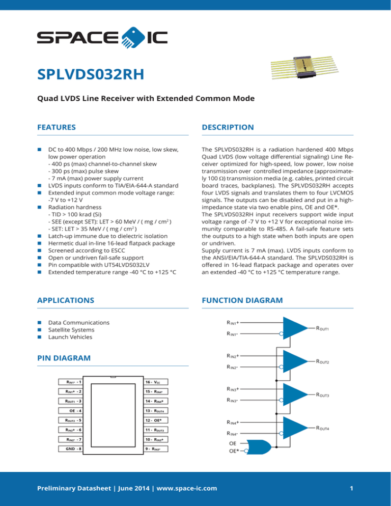
The SPLVDS032RH is a radiation hardened 400 Mbps
Quad LVDS (low voltage differential signaling) Line Receiver optimized for high-speed, low power, low noise
transmission over controlled impedance (approximately 100 W) transmission media (e.g. cables, printed circuit
board traces, backplanes). The SPLVDS032RH accepts
four LVDS signals and translates them to four LVCMOS
signals. The outputs can be disabled and put in a highimpedance state via two enable pins, OE and OE*.
The SPLVDS032RH input receivers support wide input
voltage range of -7 V to +12 V for exceptional noise immunity comparable to RS-485. A fail-safe feature sets
the outputs to a high state when both inputs are open
or undriven.
Supply current is 7 mA (max). LVDS inputs conform to
the ANSI/EIA/TIA-644-A standard. The SPLVDS032RH is
offered in 16-lead flatpack package and operates over
an extended -40 °C to +125 °C temperature range.
FUNCTION DIAGRAM
n Data Communications
n Satellite Systems
n Launch Vehicles
PIN DIAGRAM
Preliminary Datasheet | June 2014 | www.space-ic.com
SPLVDS032RH
Quad LVDS Line Receiver with Extended Common Mode
LOGIC TABLE
OE
OE*
RIN+ - RIN-
ROUT
≥ 100 mV
H
≤ -100 mV
L
Failsafe condition
H
Don‘t Care
Disabled
Any other combination
0
1
Output Truth Table
Pin Descriptions
PIN NAME
PIN NUMBER
PIN TYPE
PIN DESCRIPTION
RIN1+, RIN1-,
RIN2+, RIN2-,
RIN3+, RIN3-,
RIN4+, RIN4-
2, 1,
6, 7,
10, 9,
14, 15
LVDS
inputs
ROUT1, ROUT2,
ROUT3, ROUT4
3, 5,
11, 13
LVCMOS
outputs
Receiver LVCMOS output pins.
OE, OE*
4, 12
LVCMOS
inputs
Receiver output enable pins. When OE is high or OE* is
low or open, the receiver outputs are enabled. When OE
is low and OE* is high, the receiver outputs are disabled.
VCC
16
Power
Power supply pin. Bypass Vcc to GND with 0.1 µF and
0.01 µF ceramic capacitors.
GND
8
Power
Ground or circuit common pin.
Non-inverting and inverting LVDS receiver input pins.
Preliminary Datasheet | June 2014 | www.space-ic.com
SPLVDS032RH
Quad LVDS Line Receiver with Extended Common Mode
Absolute Maximum Ratings (NOTE1)
VCC to GND.. . . . . . . . . . . . . . . . . . . . . . . . . . . . . . . . . . . . . . -0.3 V to +4 V
Inputs
OE, OE* to GND.. . . . . . . . . . . . . . . . . . . . -0.3 V to VCC + 0.3 V
RIN+, RIN- to GND.. . . . . . . . . . . . . . . . . . -8.0 V to VCC + 13.0 V
VID (RIN+ to RIN-).. . . . . . . . . . . . . . . . . . . . . -6.0 V to VCC + 6.0 V
Outputs
ROUT to GND.. . . . . . . . . . . . . . . . . . . . . . . . . -0.3 V to VCC + 0.3 V
16-Lead Flatpack Thermal Resistance (NOTE2)
θJC.. . . . . . . . . . . . . . . . . . . . . . . . . . . . . . . . . . . . . . . . . . . . . . . . . . 10 °C/W
TJ - Maximum Junction Temperature.. . . . . . . . . . . . +150 °C
TL - Lead Temperature (soldering, 4 s).. . . . . . . . . . +260 °C
Tstg - Storage Temperature Range.. . . . . -65 °C to +150 °C
ESD Ratings
HBM1..................................................... 8 kV
MM2.................................................... 250 V
1
2
Human Body Model, applicable standard JESD22-A114-C
Machine Model, applicable standard JESD22-A 115-A
NOTE1 Stresses beyond those listed under “Absolute Maximum Ratings” may cause permanent damage to the device. These are stress
ratings only, and functional operation of the device at these or any
other conditions beyond those indicated in the operational sections
of the specifications is not implied. Exposure to absolute maximum
rating conditions for extended periods may affect device reliability.
NOTE2 When mounted on a standard JEDEC 2-layer FR-4 board.
Recommended Operating Conditions
Symbol
Parameter
Pins
MIN
TYP
MAX
Unit
VCC
Supply voltage
VCC
3.0
3.3
3.6
V
VIH
High-level input voltage
OE, OE*
2.0
VCC
V
VIL
Low-level input voltage
OE, OE*
0
0.8
V
VID
Differential input voltage
RIN+, RIN-
0.1
1
V
VIN
Input voltage
RIN+, RIN-
-7
12
V
TA
Operating free-air-temperature All
25
125
°C
TYP
MAX
Unit
-40
0.35
Electrical Characteristics
Recommended operating conditions, TA = 25 °C, VCC = 3.3V, unless otherwise specified.
Symbol
Parameter
Conditions
MIN
LVCMOS Input Specifications (OE, OE* pins)
VIH
High-level input voltage
2.0
VCC
V
VIL
Low-level input voltage
GND
0.8
V
IIH
High-level input current
VCC = 3.6 V
VIN = 3.6 V
-10
10
µA
IIL
Low-level input current
VCC = 3.6 V
VIN = 0 V
-10
10
µA
VCL
Input clamp voltage (NOTE4)
ICL = -18 mA, VCC = 0 V
-1.5
Preliminary Datasheet | June 2014 | www.space-ic.com
-0.9
V
SPLVDS032RH
Quad LVDS Line Receiver with Extended Common Mode
Electrical Characteristics (CONTINUED)
Over recommended operating conditions, TA = 25 °C, VCC = 3.3V, unless otherwise specified.
Symbol
Parameter
Conditions
MIN
TYP
MAX
Unit
IOH = -0.4 mA,
VID = 200 mV
2.7
3.2
V
IOH = -0.4 mA,
input open
2.7
3.2
V
LVCMOS Output Specifications (ROUT pins)
VOH
VOL
IOS
IOZ
Output high voltage
Output low voltage
Output short circuit current
(NOTE3), (NOTE5)
Output High-Z current
IOL = 2 mA,
VID = -200 mV
0.05
0.25
V
Enabled, VOUT = 0 V
-50
-100
mA
10
µA
100
mV
Disabled,
VOUT = 0 V or VCC
-10
LVDS Input Specifications (RIN+, RIN- pins)
VTH
Differential input high
threshold
VTL
Differential input low
threshold
VID
Differential input voltage
VICM
Input common mode voltage
IIN
CIN
Input current,
VCC = 0 or 3.6 V
Input capacitance (NOTE4)
0
VICM = -7.0 V to 12.0 V
(NOTE6)
-100
0
0.1
0.35
mV
1
V
VID = 100 mV
-7.0
12.0
V
0 V ≤ VIN+ ≤ 2.4 V,
VIN- = 1.2 V
-15
10
µA
-4 V ≤ VIN+ ≤ 6.4 V,
VIN- = open
-50
50
µA
-7 V ≤ VIN+ ≤ 12 V,
VIN- = open
-85
130
µA
RIN+ or RIN- to GND
4
pF
Power Supply Current Specifications
ICC
Power supply current
OE = 1 or OE* = 0,
Not switching
5
7
mA
ICCZ
Power supply current with
disabled outputs
OE = 0 and OE* = 1
1
2
mA
NOTE3 Current into device pin is defined as positive. Current out of the device is defined as negative.
All voltages are referenced to ground, unless otherwise specified.
NOTE4 This specification is not production tested and is guaranteed by design simuiations.
NOTE5 Output short circuit current (IOS) is specified as magnitude only. The minus sign indicates direction anly.Only one output should be shorted at a time, do not
exceed maximum junction temperature specification. Specified for momentary short condition durations only.
NOTE6 Recommended operating conditions for the RIN+ and RIN- pins is over the range of -7.0 V to 12.0 V. Therefore, caution should be taken not to exceed these
values or the maximum Differential input voltage of 1.0 V.
Preliminary Datasheet | June 2014 | www.space-ic.com
SPLVDS032RH
Quad LVDS Line Receiver with Extended Common Mode
SWITCHING Characteristics
Over recommended operating conditions, TA = 25 °C, VCC = 3.3V, unless otherwise specified.
Symbol
Parameter
Conditions
MIN
TYP
MAX
Unit
1.3
2.1
3.3
ns
1.3
2.1
3.3
ns
0.35
1
ns
0.3
1
ns
50
300
ps
100
400
ps
1.5
ns
LVDS AC Specifications (NOTES 7, 8, 9)
tPLH
Propagation delay, low-to-high
tPHL
Propagation delay, high-to-low
tr
Rise time
tf
Fall time
tSK(p)
Pulse skew (NOTE10)
tSK(c-c)
Channel-to-channel skew (NOTE11)
tSK(p-p)
Part-to-part skew (NOTE12)
tPLZ
Disable time, low-to-high Z
tPHZ
Disable time, high-to-high Z
tPZL
CL = 15 pF,
VID = 200 mV,
VICM = 1.2 V
(NOTE14)
Figures 1 and 2
8
14
ns
8
14
ns
Enable time, high Z-to-low
RL = 2 kW,
CL = 15 pF,
VID = 200 mV,
VICM = 1.2 V
8
14
ns
tPZH
Enable time, high Z-to-high
Figures 3 and 4
8
14
ns
fMAX
Maximum operating frequency
(NOTE14)
(NOTE13, NOTE14)
200
MHz
NOTE7 Generator output characteristics (unless otherwise specfied): f = 1 MHz, Z0 = 50W, tr < 1 ns, tf < 1 ns.
NOTE8 All Input voltages are for one channel unless otherwise specified. Other inputs are set to GND.
NOTE9 Switching Characteristic specifications are not production tested and are guaranteed by statistical analysis of characterization data.
NOTE10 tSK(p), pulse skew, is the magnitude difference in propagation delay time between the positive going edge and the negative going edge of the same channel
(tSK(p) = |tPLH - tPHL|).
NOTE11 tSK(c-c), channel-to-channel skew, is the difference in propagation delay time between channels on the same device at any operating temperature and supply
voltage.
NOTE12 tSK(p-p), part-to-part skew, is the difference in propagation delay time between devices operating at the same power supply voltage and within 5°C of each
other within the operating temperature range.
NOTE13 Generator output characteristics for the fMAX: Z0 = 50W, tr = tf < 1 ns, 50% duty cycle, 1.05 V to 1.35 V peak to peak. Output criteria: 60% / 40% duty cycle,
VOL (max 0.4 V), VOH (min 2.7 V).
NOTE14 The capacitive Ioad CL, includes test fixture, probe and lumped capacitance.
Preliminary Datasheet | June 2014 | www.space-ic.com
SPLVDS032RH
Quad LVDS Line Receiver with Extended Common Mode
TEst circuits and timing diagrams
Figure 1. Receiver Propagation Delay and Transition Time Test Setup
Figure 2. Receiver Propagation Delay and Transition Time Waveforms
Preliminary Datasheet | June 2014 | www.space-ic.com
SPLVDS032RH
Quad LVDS Line Receiver with Extended Common Mode
TEst circuits and timing diagrams (continued)
Figure 3. Receiver High-Z Delay Test Setup
Figure 4. Receiver High-Z Delay Test Waveforms
Preliminary Datasheet | June 2014 | www.space-ic.com
SPLVDS032RH
Quad LVDS Line Receiver with Extended Common Mode
Application information
ABOUT LVDS
Due to bandwidth and power consumption, high speed communication links usually use differential signaling.
In this area LVDS provides an outstanding performance
to power ratio: It offers a high bandwidth at very low
power consumption and low EMI. Therefore it is used
extensively for audio and video transmission, ASIC and
FPGA I/O, sensor data transmission, clock distribution
and a lot more signaling tasks.
COMMON MODE
POSSIBLE SOLUTION: AC COUPLING?
Having a look at a transmission line, usually there will
be two grounds, one transmitter ground potential and
one receiver ground potential. Defined by standard
LVDS specification, the receiver input signal has to be
between 0 and 2.4 Volts. Taking into account the typically at 1.2 Volts centered LVDS signal with a standard
400 millivolt differential signal this results in a maximum ground shift or noise margin of plus/minus 1 Volt.
This means that steady-state differences as well as momentary shifts have to be lower than 1 Volt in absolute
value. Usually this is enough margin, but under noisy
conditions, at long distances or inadequate ground connection this may cause data transfer errors.
One possibility to eliminate common mode differences
caused by ground potential issues is the use of coupling
capacitors on both channels of the differential pair. But
there is a big constraint: Capacitive coupling is only convenient for DC balanced data. This means that the data
has to have an equal number of ones and zeros. But
generally this is not the case for non-coded data, audio,
video, sensor or control signals. And if the data would
be coded in order to get a balanced signal, this would
have an impact on the bandwidth. In case of 8b/10b coding the net data rate will decrease by 20%.
GROUND BOUNCE AND GROUND DRIFT
In noisy environments and applications with known
common mode issues usually the RS-485/422 is used
due to its large swing differential standard which guarantees communication at common modes of -7 to +12
Volts. Its disadvantages are the low data rate and the
poor bandwidth to power and EMI performance.
Large switching currents in an electrical system may result in a momentary voltage drop in supply voltage and/
or in a local raise of the ground potential. In terms of the
instantaneous ground potential shift this behaviour is
known as ground bounce. This reaction to high currents
may be reduced by proper design and size of ground
and supply planes and the use of low resistive decoupling capacitors, but they cannot be eliminated totally.
Another effect in this context is a steady-state potential difference between ground connections: Each connection generates a voltage drop which follows Ohm‘s Law
(U = R * I). As a result the ground potential difference
between a module and the main ground plane rises linearly with current and terminal resistance. Since the
terminal resistance may increase by aging, the ground
potential of the connected module may drift more and
more resulting in a higher steady-state potential difference. In both situations, ground bounce and ground
drift, the common mode difference between transmitter and receiver may exceed the specified +/- 1 Volt defined by the LVDS standard resulting in communication
errors or even link interruption. These effects have already been reported in Avionics, Industrial applications,
by telecommunication companies and automobile manufacturers.
Figure 5. GND-potential difference
RS-485
SPLVDS: COMBINING THE ADVANTAGES
Having a look at the LVDS standard, the noise margin
may be sufficient on single PCBs or in small boxed systems. But in noisy environments or larger distributed
systems or box-to-box communication, the small +/-1
V common mode window potentially leads to communication problems, particularly over the lifetime of the
system. RS-485 offers a much better noise margin but
shows very poor performance regarding power consumption, speed and EMI. The new Space IC SPLVDS series combines the benefits of LVDS and RS-485: It‘s fully
compatible with the LVDS standard in terms of signal
levels, speed, power and EMI, showing the same pinout
and footprint as competitor devices. Additionally it provides an extended common mode of -7 to +12 Volt what
finally makes it a perfect choice for harsh environments.
Also it works as a high-performance replacement for
RS-485 applications.
Preliminary Datasheet | June 2014 | www.space-ic.com
SPLVDS032RH
Quad LVDS Line Receiver with Extended Common Mode
Package Dimension (16-LEAD FLATPACK)
Important NOTICE
The information contained in this document is believed to be accurate at the time of printing. Space IC reserves
the right to make changes to its products or specifications without notice, however, and assumes no responsibility
or liability for the use of its products; nor does the purchase, lease, or use of a product or service from Space IC
convey a license under any patent rights, copyrights, trademark rights, or any other of the intellectual rights of
Space IC or of third parties. Please visit our website for the most recent revision of this datasheet or contact info@
space-ic.com. Customers are responsible for their products and applications using Space IC products.
Resale of Space IC products or services with statements different from or beyond the parameters stated by Space
IC for that product or service voids all express and any implied warranties for the associated Space IC product or
service. Space IC is not responsible or liable for any such statements.
© 2014 Space IC GmbH. All rights reserved. Information and data in this document are owned by Space IC and may
not be edited, reproduced or redistributed in any way without written consent from Space IC.
Preliminary Datasheet | June 2014 | www.space-ic.com


