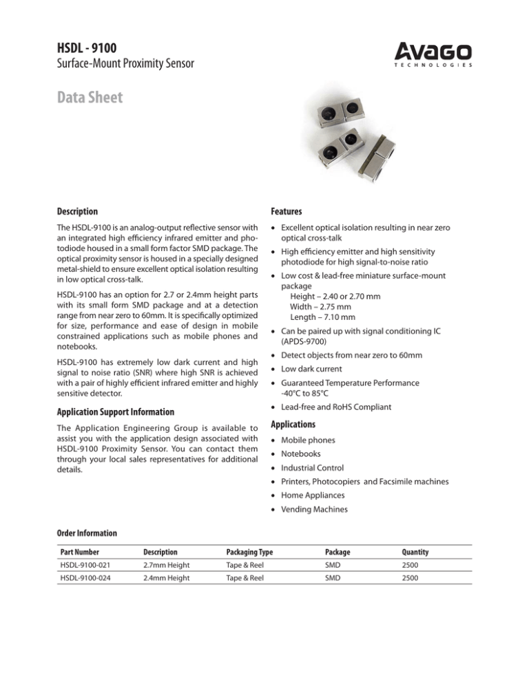
HSDL - 9100
Surface-Mount Proximity Sensor
Data Sheet
Description
Features
The HSDL-9100 is an analog-output reflective sensor with
an integrated high efficiency infrared emitter and photodiode housed in a small form factor SMD package. The
optical proximity sensor is housed in a specially designed
metal-shield to ensure excellent optical isolation resulting
in low optical cross-talk.
x Excellent optical isolation resulting in near zero
optical cross-talk
HSDL-9100 has an option for 2.7 or 2.4mm height parts
with its small form SMD package and at a detection
range from near zero to 60mm. It is specifically optimized
for size, performance and ease of design in mobile
constrained applications such as mobile phones and
notebooks.
HSDL-9100 has extremely low dark current and high
signal to noise ratio (SNR) where high SNR is achieved
with a pair of highly efficient infrared emitter and highly
sensitive detector.
x High efficiency emitter and high sensitivity
photodiode for high signal-to-noise ratio
x Low cost & lead-free miniature surface-mount
package
Height – 2.40 or 2.70 mm
Width – 2.75 mm
Length – 7.10 mm
x Can be paired up with signal conditioning IC
(APDS-9700)
x Detect objects from near zero to 60mm
x Low dark current
x Guaranteed Temperature Performance
-40°C to 85°C
x Lead-free and RoHS Compliant
Application Support Information
The Application Engineering Group is available to
assist you with the application design associated with
HSDL-9100 Proximity Sensor. You can contact them
through your local sales representatives for additional
details.
Applications
x Mobile phones
x Notebooks
x Industrial Control
x Printers, Photocopiers and Facsimile machines
x Home Appliances
x Vending Machines
Order Information
Part Number
Description
Packaging Type
Package
Quantity
HSDL-9100-021
2.7mm Height
Tape & Reel
SMD
2500
HSDL-9100-024
2.4mm Height
Tape & Reel
SMD
2500
Block Layout
Pins Configuration Table
Photodiode
LED
1
LED_A
4
DET_K
2
LED_K
3
DET_A
Pin
Symbol
Description
Notes
1
LED_A
LED Anode
1
2
LED_K
LED Cathode
-
3
DET_A
Photodiode Anode
-
4
DET_K
Photodiode Cathode
-
TOP VIEW
Notes:
Voltage to supply across the LED; VLED
Figure 1. Block Layout of HSDL-9100
Absolute Maximum Ratings (Ta=25°C)
Ratings
Parameter
Emitter
Continuous Forward Current
Coupled
Total Power Dissipation (refer to Figure 1)
Operating Temperature
Storage Temperature
Reflow Soldering Temperature
Symbol
Min.
Max
Units
IDC
-
100
mA
PTOT
TOP
TSTG
TSOL
-40
-40
-
165
+85
+100
260
mW
°C
°C
°C
Electrical-Optical Characteristics (Ta=25°C)
Ratings
Parameter
Symbol
Test Condition
Min
Typ
Max
Units
VF
VR
lp
Dp
IF = 100mA
IR = 10PA
IF = 20mA
IF = 20mA
5
-
1.50
940
50
1.65
-
V
V
nm
nm
Detector
Dark Current
Forward Voltage
Reverse Breakdown Voltage
IDark
VF
VBR
VR = 10V, L** = 0
IF = 10mA , L=0
IR = 100uA, L = 0
0.5
-
2
-
10
1.3
35
nA
V
V
Coupled
Output Current
Peak Output Distance
Operating Cross Talk Current
Rise Time (LED)
Fall Time (LED)
Rise Time (Photodiode)
Fall Time (Photodiode)
IO
DO
IFD
TRL
TFL
TRD
TFD
Refer to Fig 2
Refer Note 1
Refer to Fig 3
RL = 50:
RL = 50:
RL = 5.1K:
RL = 5.1K:
-
10
5
50
50
6
6
200
-
PA
mm
nA
ns
ns
Ps
Ps
Emitter
Forward Voltage
Reverse Voltage
Peak Wavelength
Spectrum Width of Half Value
** L = 0 (zero light condition)
Note:
1. ILed = 300mA Pulse, 5% Duty Cycle (Kodak 18% Reflectance Gray Card)
2
Output Current Test Condition (Ta=25°C)
Dark Current Test Condition (Ta=25°C)
LIGHT SEALED DARK BOX
D
KODAK GRAY CARD
18% REFLECTION
PHOTODIODE
LED
PHOTODIODE
LED
IF
IO
IF
IDARK
Figure 2.
Test Condition used are D = 5mm 18% Gray Card,
ILED = 300mA Pulse, 5% Duty Cycle
Figure 3.
Test Condition used are ILED = 300mA Pulse, 5% Duty Cycle
Response Time Test Condition (Ta=25°C)
5mm
KODAK GRAY CARD
18% REFLECTION
INPUT
LED
PHOTODIODE
90%
IF
IO
R LED
PULSE
GENERATOR
RL
OUTPUT
10%
SCOPE
TR
TF
Figure 4. Response Time Test Condition
Typical Radiation Profile for HSDL-9100
1.2
1.1
1.0
0.9
0.8
0.7
0.6
0.5
0.4
0.3
0.2
0.1
0.0
-90 -80 -70 -60 -50 -40 -30 -20 -10 0 10 20 30 40 50 60 70 80 90
Angle (degree)
1.1
1.0
0.9
0.8
0.7
0.6
0.5
0.4
0.3
0.2
0.1
0.0
-90 -80 -70 -60 -50 -40 -30 -20 -10 0 10 20 30 40 50 60 70 80 90
3
Normalized Responsivity
HSDL-9100 Typical Photodiode Angular Responsivity Profile
Normalized radiant intensity
HSDL-9100 Typical LED Angular Emitting Profile
Angle (degree)
Typical Characteristics
Power Dissipation Vs Temperature
200
90
180
80
160
70
140
60
120
Power (mW)
Forward Current
LED Forward Current Vs Temperature
100
50
40
100
80
30
60
20
40
10
20
0
0
0
10
20
30
40
50
60
70
80
0
90
10
20
30
Temperature (˚C)
LED Forward Current Vs Forward Voltage @ Across Temperature
60
70
80
90
(Photodiode) Forward Current Vs Forward Voltage@Across Temp
E-3
0.12
.0
20
25
-25
85
0.1
25
-25
85
1
-3
.0E
0
10
0.08
Forward Current (A)
Forward Current (A)
40
50
Temperature (˚C)
0.06
0.04
-3
.0E
80
-3
.0E
60
-3
.0E
40
0.02
-3
.0E
20
0
0
0.2
0.4
0.6
0.8
1
1.2
1.4
+0
.0E
1.6
0
00
Forward Voltage (V)
0
Forward Current (A) Vs Temperature (degC) @Vcc=1V and 1.3V
0.1
+3
0.09
0.08
0.06
1V
0.05
1.3V
0.04
0.03
0.02
0.01
0
-40
-20
0
20
40
Temperature (˚C)
4
60
80
100
Response Time (us)
Forward Current (A)
0.07
E
1.0 0
+
.0 0E 0
90 E+
0.0
80 E+0
0.0
70 E+0
0.0
60 E+0
0.0
50 E+0
0.0
40 E+0
0.0
30 E+0
0.0
20 E+0
0.0
10 E+0 0.1
0.0
00
0.2
0.4
0.6
0.8
1
Forward Voltage (V)
1.2
1.4
1.6
(Photodiode) Rise/Fall Time Vs Load Resistance@Room Temp,
ILED=300mA Pulse
(Rise
(Fall)
Mean
(Fall)
1
10
100
Load Resistance (kohm)
1000
10000
Output Voltage vs Distance @ Room Temp and RL = 100K
Ohm ILED = 100mA, 200mA and 300mA Pulse
1.0
E-6
(Photodiode) Dark Current Vdet = 3/6/9V vs Across Temperature
3
E+
1.0
3V
300mA
200mA
100mA
6V
1.0
E-9
Dark Current (A)
10
10
0.0
.0E
E-9
-9
Output Voltage (mV)
9V
0
E+
0.0
10
90
+0
.0E
10
0
-40
-20
0
20
40
60
80
100
E+
1.0
2
3
Temperature (˚C)
3mm
4mm
5mm
900
Output Voltage (mV)
800
10 20 30 40 50 60 80 100 120 300 400 450
Distance (mm)
The diagram below illustrates the explanation of edge
distance. Edge detection is labeled as D in the diagram
below.
Output Voltage Vs Edge Distance @ Room Temp
and RL=100K Ohm ILED=300mA, D=3/4/5mm
1000
5
700
600
500
400
300
18% Reflection
Gray Card
200
100
0
-10
-8
-6
-4
-2
0
Edge Distance (mm)
2
4
6
Distance = D(mm)
LED
Distance = -D(mm)
PIN
5mm
5
HSDL-9100 Package Outlines
3.88
2.75
2.35
1.375
R0
R1
.9 0
Mounting Centre
2.48
3.55
Tx
0.10
Rx
0.10
0.8
2.7
6.9
0.05
0.05
7.10
0.625
2.35
3
1
4
Pin 1 - LED Anode
Pin 2 - LED Cathode
Pin 3 - Photodiode Anode
Pin 4 - Photodiode Cathode
0.6
1.1
2.35
2
2
Photodiode
direction mark
Figure 5a. HSDL-9100-021 Package dimensions
3.88
2.75
2.35
1.375
R1
R0
.9
Mounting Centre
2.48
Rx
3.55
Tx
0.1
0.1
0.8
2.4
6.9
0.05
0.05
2.35
0.625
7.10
3
1
4
Photodiode
direction mark
Figure 5b. HSDL-9100-024 Package dimensions
6
2
0.6
1.1
2.35
2
Pin 1 - LED Anode
Pin 2 - LED Cathode
Pin 3 - Photodiode Anode
Pin 4 - Photodiode Cathode
1.55±0.05
1.75
Rx Anode
Tx Cathode
2±0.1
4±0.1
B
7.5
Rx Cathode
Tx Anode
1.5
2.78±0.07
16
7.35±0.1
B-B Section
0.35
5˚ (MAX)
HSDL-9100-021/024 Tape and Reel Dimensions
8±0.1
A
A
2.95±0.1
B
PROGRESSIVE DIRECTION
UNIT: MM
EMPTY
PARTS MOUNTED
LEADER
(400 mm MIN.)
(40 mm MIN.)
EMPTY
(40 mm MIN.)
OPTION #
"B"
"C"
QUANTITY
001
178
60
500
021
330
80
2500
UNIT: mm
DETAIL A
2.0 ± 0.5
B
C
16.4
+2
0
13.0 ± 0.5
R 1.0
LABEL
21 ± 0.8
DETAIL A
2.0 ± 0.5
Figure 6. Tape and Reel Dimensions
7
HSDL-9100 Moisture Proof Packaging
Baking Conditions Chart
All HSDL-9100 options are shipped in moisture proof
package. Once opened, moisture absorption begins.
Units in A Sealed
Moisture-Proof
Package
This part is compliant to JEDEC Level 3.
Baking Conditions
If the parts are not stored in dry conditions, they must
be baked before reflow to prevent damage to the parts.
Package
Temp
Time
In reels
60 °C
t 48hours
100 °C
t4hours
125 °C
t 2 hours
In bulk
Package Is
Opened (Unsealed)
Environment
less than 30 deg C,
and less than
60% RH
Baking should only be done once.
Yes
Recommended Storage Conditions
Storage Temperature
10°C to 30°C
Relative Humidity
below 60% RH
No Baking
Is Necessary
Yes
Time from unsealing to soldering
No
After removal from the bag, the parts should be soldered
within seven days if stored at the recommended storage
conditions.
No
Perform Recommended
Baking Conditions
Figure 7. Baking conditions chart
8
Package Is
Opened less
Than 168 hours
Recommended Reflow Profile
MAX 260°C
T - TEMPERATURE (°C)
255
R3
230
217
200
180
150
120
R2
R4
60 sec to 120 sec
Above 217°C
R5
R1
80
25
0
50
P1
HEAT
UP
Process Zone
100
150
P2
SOLDER PASTE DRY
Symbol
200
P3
SOLDER
REFLOW
'T
250
300
t-TIME
(SECONDS)
P4
COOL DOWN
Maximum 'T/'time
or Duration
Heat Up
P1, R1
25°C to 150°C
3°C/s
Solder Paste Dry
P2, R2
150°C to 200°C
100s to 180s
Solder Reflow
P3, R3
P3, R4
200°C to 260°C
260°C to 200°C
3°C/s
-6°C/s
Cool Down
P4, R5
200°C to 25°C
-6°C/s
> 217°C
60s to 120s
Time maintained above liquidus point , 217°C
Peak Temperature
Time within 5°C of actual Peak Temperature
Time 25°C to Peak Temperature
The reflow profile is a straight-line representation of
a nominal temperature profile for a convective reflow
solder process. The temperature profile is divided into
four process zones, each with different 'T/'time temperature change rates or duration. The 'T/'time rates or
duration are detailed in the above table. The temperatures are measured at the component to printed circuit
board connections.
In process zone P1, the PC board and component pins are
heated to a temperature of 150°C to activate the flux in
the solder paste. The temperature ramp up rate, R1, is
limited to 3°C per second to allow for even heating of
both the PC board and component pins.
Process zone P2 should be of sufficient time duration (100
to 180 seconds) to dry the solder paste. The temperature
is raised to a level just below the liquidus point of the
solder.
260°C
-
> 255°C
20s to 40s
25°C to 260°C
8mins
Process zone P3 is the solder reflow zone. In zone P3, the
temperature is quickly raised above the liquidus point
of solder to 260°C (500°F) for optimum results. The
dwell time above the liquidus point of solder should be
between 60 and 120 seconds. This is to assure proper
coalescing of the solder paste into liquid solder and the
formation of good solder connections. Beyond the recommended dwell time the intermetallic growth within
the solder connections becomes excessive, resulting in
the formation of weak and unreliable connections. The
temperature is then rapidly reduced to a point below
the solidus temperature of the solder to allow the solder
within the connections to freeze solid.
Process zone P4 is the cool down after solder freeze.
The cool down rate, R5, from the liquidus point of the
solder to 25°C (77°F) should not exceed 6°C per second
maximum. This limitation is necessary to allow the PC
board and component pins to change dimensions evenly,
putting minimal stresses on the component.
It is recommended to perform reflow soldering no more
than twice.
9
Appendix A: HSDL-9100 SMT Assembly Application Note
Recommended Metal solder Stencil Aperture
Table 1. Combinations of metal stencil aperture and metal
stencil thickness
0.6
2.75
0.5
0.6
7.7
7.1
0.6
It is recommended that only a 0.152 mm (0.006 inch) or
a 0.127 mm (0.005 inch) thick stencil be used for solder
paste printing. This is to ensure adequate printed solder
paste volume and no shorting. See Table 1 below the
drawing for combinations of metal stencil aperture and
metal stencil thickness that should be used. Aperture
opening for shield pad is 3.05 mm x 1.1 mm as per land
pattern.
0.525
Recommended land pattern
2.1
2.4
Solder / stencil opening for each pad is 2.4mm x0.6mm
Figure 10. Land Pattern
Stencil
Aperture size (mm)
thickness,
t (mm)
Length,
l
Width,
w
0.152
1.60+/-0.05
0.55+/-0.05
0.127
1.92
0.55+/-0.05
Apertures as per
Land Dimensions
t
l
w
Adjacent Land Keep out and Solder Mask Areas
Adjacent land keep out is the maximum space occupied
by the unit relative to the land pattern. There should be
no other SMD components within this area. The minimum
solder resist strip width required to avoid solder bridging
adjacent pads is 0.2mm.It is recommended that two
fiducial crosses be placed at mid length of the pads for
unit alignment. Also do take note that there should not
be any electrical routing with the component placement
compartment.
Figure 11. Solder stencil aperture
k
Component placement
j
h
Note:
Wet/Liquid Photo-imaginable solder resist/mask is recommended
Mounting Center
Solder Mask
Solder Pad, Mask and Metal Stencil
l
Metal stencil for
solder paste printing
Stencil Aperture
Land Pattern
Dim.
mm
h
4.15
l
11
k
5.5
j
3.5
Figure 12. Keep-out area
Solder Mask
PCBA
Figure 9. Stencil and PCBA
10
Appendix B: General Application Guide for the HSDL-9100
Description
Interface to the Recommended I/O chip
The Proximity sensor has several possible applications for
multimedia product, Automation, and Personal handled.
The proximity sensor is basically made up of the emitter
(infrared LED) and detector (photodiode). The block
diagram of the sensor is shown in Figure 13. The emitter
will emit IR light pulse. This light travels out in the field
of view and will either hit an object or continue. No light
will be reflected when no object is detected. On the other
hand, the detector will detect the reflected IR light when
it hits the object.
The HSDL-9100 is general interface with the GPIO pin of
the controller chipset. The LED_A, pin1 is connected to
the PWM port alternatively the external timer circuitry
can be used to drive the LED. The DET_K, pin 4 is interface
to the signal conditioning before driving the GPIO port.
Figure 14 shows the hardware reference design with
HSDL-9100.
Photodiode
3
4
Photodiode
anode
Photodiode
cathode
2
1
LED
anode
LED
cathode
LED
Figure 13. Proximity sensor block diagram
(refer to Pins Configuration Table)
Key Pad
STN/TFT LCD Panel
LCD Control
Touch Panel
Peripherial
interface
A/D
IrDA
interface
Mobile Application
chipset
Memory Expansion
Logic Bus Driver
Memory I/F
Baseband
controller
ROM
Power Management
IR Transceiver
GPIO
AC97
sound
PCM Sound
I2S
Audio Input
PWM
Antenna
FLASH
*IR LED driver
SDRAM
Signal Conditional
*
The LED can be driven by the PWM output or the external timer circuitry.
Figure 14. Mobile Application Platform
11
HSDL-9100
The next section discusses interfacing configuration with
general processor including the recommended signal
conditional circuitry.
The DET_A pin of HSDL-9100 is connected to the filter
circuit then to the comparator before interfacing with
the GPIO pin. The filter circuit is implement to provide
the ambient light filter. The PWM is pulse to drive the
LED_K pin alternative the external timer 555 can also be
replaced. The detector distance can be varies with the
increase/decrease of the LED current supply.
Interfacing circuitry with signal conditional circuitry
VCC
HSDL-9100
DETK
DETA
LEDA
LEDK
PWM
VCC
220 Ω
VCC
36 KΩ
BC848
22 KΩ
220 pf
10 Ω
BC846B
24 KΩ
GND
GND
1 MΩ
VCC
GND
47 kΩ
GPIO
300 Ω
controller chipset
GND
Signal conditioning circuitry
Figure 15. HSDL9100 configuration with controller chipset
12
Appendix C: Recommended window and light guide for HSDL-9100
x Using opaque material of light pipes with two holes as
light path. The structure need to be carefully designed
to minimize the signal loss and crosstalk. (See option 3)
Close to the window
Material #
Light
Transmission
Haze
Refractive
Index
Lexan 141
88%
1%
1.586
Lexan 920A
85%
1%
1.586
Lexan 940A
85%
1%
1.586
Note:
920A and 940A are more flame retardant than 141.
Recommended Dye: Violet #21051 (IR transmissant above 625 nm)
For product information and a complete list of distributors, please go to our web site: www.avagotech.com
Avago, Avago Technologies, and the A logo are trademarks of Avago Technologies in the United States and other countries.
Data subject to change. Copyright © 2005-2009 Avago Technologies. All rights reserved. Obsoletes AV02-0779EN
AV02-2259EN - November 26, 2009
Flat Window (Transmission rate >85%)
Recommended Plastic Materials:
Photodiode
Photodiode
Option 3
LED
Flat Window (Transmission rate >85%)
Recommended Window Material
Almost any plastic material will work as a window material. Polycarbonate is recommended. The surface finish
of the plastic should be smooth, without any texture.
The thickness of the window material is recommended
to be less than 0.5mm. An IR filter dye may be used in
the window to make it look black to the eye but the total
optical loss of the window should be 10% or less for best
optical performance. Light loss should be measured at
875nm. The recommended plastic materials for use as a
cosmetic window are available for General Electric Plastics.
Option 2
Option 1
LED
x Using separate pieces of light guide bonded together
for emitter and photo sensor respectively. Insert a baffle
in between the two light guides. (See option 4)
Photodiode
Photodiode
x Using baffle in between emitter and detector will
reduce the crosstalk caused by bottom surface. It is recommended to extend the baffle into the flat window as
to reduce the crosstalk caused by top surface too. (See
option 2)
Flat Window (Transmission rate >85%)
x Put the optical sensor close to the window material.
(See option 1)
LED
Flat Window (Transmission rate >85%)
LED
Some constraints on the design and position of the window are required so that the cross talk from the emitter
to the photodiode is minimized. Four recommendations
of window design are suggested as below:
Option 4
