Schottky Diode: Band Diagrams, Characteristics, and Applications
advertisement
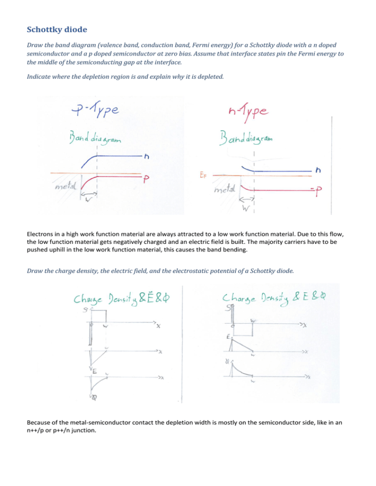
Schottky diode Draw the band diagram (valence band, conduction band, Fermi energy) for a Schottky diode with a n doped semiconductor and a p doped semiconductor at zero bias. Assume that interface states pin the Fermi energy to the middle of the semiconducting gap at the interface. Indicate where the depletion region is and explain why it is depleted. Electrons in a high work function material are always attracted to a low work function material. Due to this flow, the low function material gets negatively charged and an electric field is built. The majority carriers have to be pushed uphill in the low work function material, this causes the band bending. Draw the charge density, the electric field, and the electrostatic potential of a Schottky diode. Because of the metal-semiconductor contact the depletion width is mostly on the semiconductor side, like in an n++/p or p++/n junction. Draw the band diagram in forward bias. Of the current transport mechanisms we discussed in course (drift, diffusion, thermionic emission, and tunneling) which are dominant in a forward biased Schottky diode. Which are dominant in a reverse biased diode? Why? Picture (a) shows the n- Type shottky contact under equilibrium conditions. The band bending is caused by the difference in work functions of the two materials. Electrons have to be thermally activated to overcome the barrier. This carrier transport is called “Thermionic emission”. No current is flowing, because the current from the metal side and the current from the semiconductor side cancel each other out. Picture (b) shows how the bands are bending when the contact is forward biased. As we can see is the barrier on the semiconductor side, which the electrons have to overcome, much smaller than under equilibrium conditions – The current from the semiconductor side is now the bigger than the one from the metal - current is flowing. Picture (c) shows a strong forward biased shottky junction. Under this condition very much current is flowing. One effect in this mode is, that holes are able to tunnel trough the barrier, recombine with electrons in the depletion region and emit a photon. In a reverse biased junction also thermionic emission dominates. But in this case the current from the semiconductor side is zero. And only the current from the metal side is present. Draw the current voltage characteristics for a Schottky diode. What is the formula? How is this formula derived? The current is transported via thermionic emission. All other currents like diffusion can be neglected, because the ration between them and thermionic emission is very small. The current flowing depends on two parts: the one which is flowing from the metal to the semiconductor minus the one which is flowing from the semiconductor to the metal. Because the current transport mechanism is thermionic emission we can insert the formulas for the currents. The majority carriers from the metal must overcome the whole barrier; the majority carriers from the semiconductor must overcome just the reduced barrier height, caused by the bias voltage. A ... Area ... Richardson constant T ... Temperature ... Barrier height ... Bias voltage Why is the nonideality factor about 1 for a Schottky diode? Because of the metal semiconductor contact, there is no recombination in the depletion region; this is the reason why the non ideality factor is about one. Compare a Schottky diode to a pn-diode. In which applications do Schottky diodes perform better than pndiodes? Schottky Diode p-n Diode Forward current due to thermionic emission (majority carrier transport) Forward current due to diffusion currents (minority carrier transport) Reverse current only due to majority carriers that overcome the barrier (less temperature dependent) Reverse current due to minority carriers diffusing to the depletion layer and drifting to the other side (strong temperature dependence) Cut-in voltage is small (about 0.3V) Cut-in voltage is large (about 0.7V) High switching speed, because of majority carrier transport. No recombination time needed! Switching speed limited by the recombination time of the injected minority carriers Ideality factor about 1 - no recombination in depletion layer Ideality factor about 1.2-2.0 due to recombination in depletion layer One application, where shottky diodes perform better than pn diodes, is in a mixer.
