STWK01
Secondary side wake-up controller
Datasheet - preliminary data
winding. The internal N-channel MOSFET (the
source connected to GND and the drain to the
OUT pin) has to be placed in parallel to the
flyback converter output diode.
SOT23 – 6L
(plastic package)
Features
• Precise voltage references: 2 V ± 1% and 2.4 V
± 2%, within temperature range
• Wide operating VDD range (from 4.5 to 20 V)
• Low consumption during burst mode: 150 µA
• OVP detection function during burst mode
• Internal 100 V N-channel MOSFET
• SOT23-6L micropackage
Applications
• Adapter/charger: mobile phone, tablet,
camcorder, shaver, emergency light, etc.
based on the primary side controller STCH01
When at a light load or no-load the main device
STCH01 enters burst mode operation and stops
switching, the wake-up controller senses at the
secondary side that there is no switching activity
and remains waiting that the output voltage
discharges down to the threshold set by an
external resistive divider connected to the sensing
pin Vsns: when the internal threshold is reached,
the wake-up controller switches on the internal
MOSFET for a short time interval: this allows to
generate a wake-up pulse across the transformer
secondary winding that, by a transformer
coupling, is transferred at the primary side across
the auxiliary winding connected to the primary
side controller STCH01. The transferred wake-up
pulse is detected by the ZCD pin of the main IC
that resumes the operation.
The device generates a wake-up pulse also in
case, during burst mode operation, it detects an
overvoltage condition on the output.
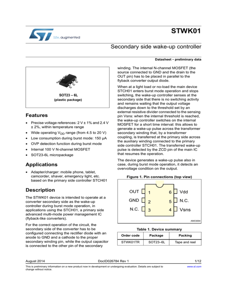
Figure 1. Pin connections (top view)
Description
The STWK01 device is intended to operate at a
converter secondary side as the wake-up
controller during burst mode operation, in
applications using the STCH01, a primary side
advanced multi-mode power management IC
(flyback-like converters).
For the correct operation of the circuit, the
secondary side of the converter has to be
configured connecting the rectifier diode with an
anode to GND and a cathode to the proper
secondary winding pin, while the output capacitor
is connected to the other pin of the secondary
August 2014
287
9GG
*1'
1&
1&
9VQV
$0
Table 1. Device summary
Order code
Package
Packing
STWK01TR
SOT23–6L
Tape and reel
DocID026784 Rev 1
This is preliminary information on a new product now in development or undergoing evaluation. Details are subject to
change without notice.
1/12
www.st.com
Contents
STWK01
Contents
1
Block diagram . . . . . . . . . . . . . . . . . . . . . . . . . . . . . . . . . . . . . . . . . . . . . . 3
2
Maximum ratings . . . . . . . . . . . . . . . . . . . . . . . . . . . . . . . . . . . . . . . . . . . . 4
3
Electrical characteristics . . . . . . . . . . . . . . . . . . . . . . . . . . . . . . . . . . . . . 5
4
Application information . . . . . . . . . . . . . . . . . . . . . . . . . . . . . . . . . . . . . . 6
5
Operation . . . . . . . . . . . . . . . . . . . . . . . . . . . . . . . . . . . . . . . . . . . . . . . . . . 7
5.1
Wake-up comparator . . . . . . . . . . . . . . . . . . . . . . . . . . . . . . . . . . . . . . . . . 7
5.2
OVP comparator . . . . . . . . . . . . . . . . . . . . . . . . . . . . . . . . . . . . . . . . . . . . . 8
6
Package information . . . . . . . . . . . . . . . . . . . . . . . . . . . . . . . . . . . . . . . . . 9
7
Revision history . . . . . . . . . . . . . . . . . . . . . . . . . . . . . . . . . . . . . . . . . . . 11
2/12
DocID026784 Rev 1
STWK01
Block diagram
Figure 2. Block diagram
9GG
287
9EXV
&/2&.DQG
/2*,&
5()
89/2
:DNHXS
FRPS
6833/<
DQG89/2
B
'5,9(
293
FRPS
B
1
Block diagram
*1'
9UHI
95RYS
9VQV
$0
Figure 3. Typical application schematic
DocID026784 Rev 1
3/12
12
Maximum ratings
2
STWK01
Maximum ratings
Table 2. Absolute maximum ratings
Symbol
Pin
VDD
6
VOUT
Parameter
Value
Unit
Device supply voltage
-0.3 to 22
V
1
OUT pin to GND voltage
-3 to 100
V
IOUT
1
Max. sink pulsed current (pulse width internally limited to 4 µs)
2.5
A
Vsns
4
Sense pin voltage
-0.3 to 3.6
V
Stressing the device above the rating listed in Table 2: Absolute maximum ratings may
cause permanent damage to the device. Exposure to absolute maximum rated conditions
may affect device reliability.
Table 3. Thermal data
Symbol
Parameter
Value
Unit
Rth j-amb
Thermal resistance, junction to ambient
250
°C/W
PTOT
Max. power dissipation at Tamb = 50 °C
0.4
W
Tjop
Junction temperature operating range
-40 to 150
Tstg
Storage temperature
-55 to 150
°C
Table 4. Pin functions
No.
Name
Function
1
OUT
The drain of the internal N-channel MOSFET: has to be connected to the cathode of the rectifier
diode at secondary side of the flyback converter. Note that, for the correct operation of the circuit,
the secondary side of the converter has to be configured connecting the rectifier diode with an
anode to GND and a cathode to the proper secondary winding terminal, while the output capacitor
is connected to the other terminal of the secondary winding.
2
GND
Return of the bias current of the device and 0 V reference for all voltages.
3
N.C.
This pin has to be connected to ground (GND).
3
GND
Return of the bias current of the device and 0 V reference for all voltages.
4
Vsns
Sensing input: the mid-point of a resistive divider from the converter output to GND should be
connected to this pin for output voltage sensing. The sensed voltage on the pin is compared to the
internal references for the wake-up and OVP function.
5
N.C.
This pin has to be connected to ground (GND).
6
VDD
Supply voltage of the device. A small bypass capacitor (0.1 µF typ.) to GND, located as close to
IC's pins as possible, might be useful to get a clean supply voltage.
4/12
DocID026784 Rev 1
STWK01
3
Electrical characteristics
Electrical characteristics
Table 5. Electrical characteristics (TJ = -25 °C to 125 °C, VDD = 5 V; unless otherwise specified)
Symbol
Parameter
Test condition
Min. Typ. Max. Unit
Internal MOSFET (between OUT and GND pins)
VDS_Max Max. operating voltage
IOFF
RDS(on)
TJ = 25 °C
100
V
Off state drain leakage
current
VDS = 100 V; TJ = 125 °C,
Vsns > Vref
15
µA
Static drain-source ON-resistance
ID = 0.5 A; TJ = 25 °C
Ω
3
Supply section
Voltage operating range
4.5
Vdd_on
Vdd turn on threshold
4.45
Vdd_off
Vdd turn off threshold
4.2
VDD
Vdd_hyst Turn on - turn off threshold hysteresis
IDD
Quiescent current
20
V
4.6
4.75
V
4.35
4.5
V
190
Vsns = 2.06 V; not switching
mV
70
150
µA
Wake-up sensing
Vref
Wake-up comparator voltage
reference
(1)V
(1)
DD
within supply range, TJ = 25 °C
VDD within supply range
VRovp
OVP comparator voltage reference
(1)V
Tpulse
Gate drive pulse width
On comparators triggering
DD
within supply range
1.99
2
2.01
1.98
2
2.02
2.35
2.4
2.45
V
4
V
µs
1. All voltages in tracking.
DocID026784 Rev 1
5/12
12
Application information
4
STWK01
Application information
Figure 4. Typical application schematic including STCH01 portion
TR
Vout
STWK01
R1
Vdd
Cout
OUT Vsns
Dout
STCH01
GND
R2
DRAIN
ZCD
Rzcd
Rf b
AUX
AM03697
6/12
DocID026784 Rev 1
STWK01
5
Operation
Operation
During the burst mode this device operates at the converter secondary side as the wake-up
controller, in flyback-like applications using the STCH01, a primary side advanced multimode power management IC.
For the correct operation of the circuit, the secondary side of the converter has to be
configured connecting the output rectifier diode with an anode connected to GND and
a cathode connected to the proper secondary winding terminal of the flyback transformer,
while the output filter capacitor is connected to the other terminal of the secondary winding.
In very light load or no-load conditions, when the COMP pin of the STCH01 reaches the
burst mode threshold VCOMPBM, the primary controller stops switching, entering a very low
consumption state and waiting for a wake-up signal (on the ZCD pin) from the secondary
side: as a result of an operation stop, the output voltage will start decreasing due to the
residual load.
The operation of the wake-up device (after start-up phase) is to detect the switching activity
stop and trigger the internal wake-up comparator when the output voltage is sensed below
the threshold fixed by the resistive divider connected to the sense pin Vsns and compared to
the internal reference Vref.
Referring to the block diagram in Figure 2 on page 3, the clock and logic block detects the
switching activity stop and only after this it enables the wake-up and OVP comparators.
On the comparator triggering, the internal N-channel MOSFET is turned on for a short time
(Tpulse), allowing a voltage pulse to be transferred from the secondary winding to the
auxiliary winding, through the transformer coupling. The resulting pulse train on the ZCD pin
is detected by the primary side controller that resumes the operation. The IC implements
also a snooze function: after releasing the first pulse, in case no switching activity is
detected within a snooze time (22 µsec. typ.), it releases a second wake-up pulse in order to
increase the robustness of the communication between primary and secondary controllers.
The complementary operation of the primary and secondary ICs during very light load or noload conditions allows extremely low power consumption, making the architecture suitable
for those charger applications where 5-star requirements in the no-load have to be overexceeded.
5.1
Wake-up comparator
The wake-up threshold is set by the R1 - R2 divider and has to be selected lower than the
nominal output voltage (set at the primary side, through the resistive divider connected to
the ZCD pin of the STCH01), but of course above the minimum allowed value in the
specification for the output.
Once chosen this threshold Vo_wake and the resistor R2 of the divider, the other resistor R1
can be calculated as follows:
Equation 1
V o wake
R1 = --------------------- – 1 R2
V ref
DocID026784 Rev 1
7/12
12
Operation
5.2
STWK01
OVP comparator
During burst mode operation (when a switching operation stop is detected), the same
resistive divider R1 - R2 is also used to sense an overvoltage condition: the sensed voltage
Vsns is sent to the OVP comparator and compared to a second threshold VRovp that is set
20% higher than voltage reference Vref. As a result, the OVP comparator triggers when the
output voltage surpasses the value:
Equation 2
Vo
ovp
R1
R1
= VR ovp -------- + 1 = 1.2 • V ref -------- + 1
R2
R2
and a wake-up pulse is transferred from the secondary to auxiliary winding, where it is
detected by the ZCD pin of the STCH01. Also in this case a second pulse is released, in
case no switching activity is detected within a snooze time (22 µsec. typ.).
8/12
DocID026784 Rev 1
STWK01
6
Package information
Package information
In order to meet environmental requirements, ST offers these devices in different grades of
ECOPACK® packages, depending on their level of environmental compliance. ECOPACK
specifications, grade definitions and product status are available at: www.st.com.
ECOPACK is an ST trademark.
Figure 5. SOT23-6L package outline
627/
DocID026784 Rev 1
9/12
12
Package information
STWK01
Table 6. SOT23-6L package mechanical data
Dimensions (1)
Symbol
mm.
Min.
inch
Typ.
Max.
A
0.9
A1
Typ.
Max.
1.45
0.035
0.057
0
0.1
0
0.0039
A2
0.9
1.3
0.035
0.0512
b
0.35
0.5
0.014
0.02
c
0.09
0.2
0.004
0.008
D
2.8
3.05
0.11
0.120
E
1.5
1.75
0.059
0.0689
e
0.95
0.037
H
2.6
3
0.102
0.118
L
0.1
0.6
0.004
0.024
Θ (degrees)
0°
10°
0°
10°
1. Dimensions per JEDEC MO178AB.
10/12
Min.
DocID026784 Rev 1
STWK01
7
Revision history
Revision history
Table 7. Document revision history
Date
Revision
06-Aug-2014
1
Changes
Initial release.
DocID026784 Rev 1
11/12
12
STWK01
IMPORTANT NOTICE – PLEASE READ CAREFULLY
STMicroelectronics NV and its subsidiaries (“ST”) reserve the right to make changes, corrections, enhancements, modifications, and
improvements to ST products and/or to this document at any time without notice. Purchasers should obtain the latest relevant information on
ST products before placing orders. ST products are sold pursuant to ST’s terms and conditions of sale in place at the time of order
acknowledgement.
Purchasers are solely responsible for the choice, selection, and use of ST products and ST assumes no liability for application assistance or
the design of Purchasers’ products.
No license, express or implied, to any intellectual property right is granted by ST herein.
Resale of ST products with provisions different from the information set forth herein shall void any warranty granted by ST for such product.
ST and the ST logo are trademarks of ST. All other product or service names are the property of their respective owners.
Information in this document supersedes and replaces information previously supplied in any prior versions of this document.
© 2014 STMicroelectronics – All rights reserved
12/12
DocID026784 Rev 1
