Exercise 8-1: (Problem 8.16) Develop a block diagram and an
advertisement
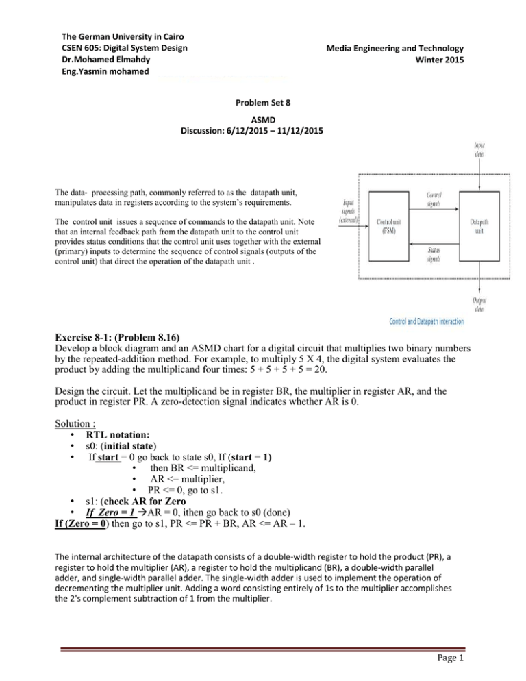
The German University in Cairo CSEN 605: Digital System Design Dr.Mohamed Elmahdy Eng.Yasmin mohamed Media Engineering and Technology Winter 2015 Problem Set 8 ASMD Discussion: 6/12/2015 – 11/12/2015 The data‐ processing path, commonly referred to as the datapath unit, manipulates data in registers according to the system’s requirements. The control unit issues a sequence of commands to the datapath unit. Note that an internal feedback path from the datapath unit to the control unit provides status conditions that the control unit uses together with the external (primary) inputs to determine the sequence of control signals (outputs of the control unit) that direct the operation of the datapath unit . Exercise 8-1: (Problem 8.16) Develop a block diagram and an ASMD chart for a digital circuit that multiplies two binary numbers by the repeated-addition method. For example, to multiply 5 X 4, the digital system evaluates the product by adding the multiplicand four times: 5 + 5 + 5 + 5 = 20. Design the circuit. Let the multiplicand be in register BR, the multiplier in register AR, and the product in register PR. A zero-detection signal indicates whether AR is 0. Solution : • RTL notation: • s0: (initial state) • If start = 0 go back to state s0, If (start = 1) • then BR <= multiplicand, • AR <= multiplier, • PR <= 0, go to s1. • s1: (check AR for Zero • If Zero = 1 AR = 0, ithen go back to s0 (done) If (Zero = 0) then go to s1, PR <= PR + BR, AR <= AR – 1. The internal architecture of the datapath consists of a double-width register to hold the product (PR), a register to hold the multiplier (AR), a register to hold the multiplicand (BR), a double-width parallel adder, and single-width parallel adder. The single-width adder is used to implement the operation of decrementing the multiplier unit. Adding a word consisting entirely of 1s to the multiplier accomplishes the 2's complement subtraction of 1 from the multiplier. Page 1 The German University in Cairo CSEN 605: Digital System Design Dr.Mohamed Elmahdy Eng.Yasmin mohamed Media Engineering and Technology Winter 2015 Page 2 The German University in Cairo CSEN 605: Digital System Design Dr.Mohamed Elmahdy Eng.Yasmin mohamed Media Engineering and Technology Winter 2015 Exercise 8-3: (Problem 8.22) The figure below shows an alternative ASMD chart for a sequential binary multiplier. Write and verify an RTL model of the system Page 3 The German University in Cairo CSEN 605: Digital System Design Dr.Mohamed Elmahdy Eng.Yasmin mohamed Media Engineering and Technology Winter 2015 Page 4 The German University in Cairo CSEN 605: Digital System Design Dr.Mohamed Elmahdy Eng.Yasmin mohamed Media Engineering and Technology Winter 2015 Page 5 The German University in Cairo CSEN 605: Digital System Design Dr.Mohamed Elmahdy Eng.Yasmin mohamed Media Engineering and Technology Winter 2015 Page 6 The German University in Cairo CSEN 605: Digital System Design Dr.Mohamed Elmahdy Eng.Yasmin mohamed Media Engineering and Technology Winter 2015 *Exercise 8-4: (Problem 8.29) An ASMD chart for a finite state machine is shown in the figure below. The register operations are not specified, because we are interested only in designing the control logic. (a) Draw the equivalent state diagram. (b) Write and verify an HDL description of the controller. Page 7 The German University in Cairo CSEN 605: Digital System Design Dr.Mohamed Elmahdy Eng.Yasmin mohamed Media Engineering and Technology Winter 2015 Solution: Page 8 The German University in Cairo CSEN 605: Digital System Design Dr.Mohamed Elmahdy Eng.Yasmin mohamed Media Engineering and Technology Winter 2015 Exercise 8-4 (Problem 8.8 ) Design a digital circuit with three 16‐bit registers AR, BR, and CR that perform the following operations: (a) Transfer two 16‐bit signed numbers (in 2’s‐complement representation) to AR and BR . (b) If the number in AR is negative, divide the number in AR by 2 and transfer the result to register CR . (c) If the number in AR is positive but nonzero, multiply the number in BR by 2 and transfer the result to register CR . (d) If the number in AR is zero, clear register CR to 0. (e) Write and verify a behavioral model of the circuit Page 9 The German University in Cairo CSEN 605: Digital System Design Dr.Mohamed Elmahdy Eng.Yasmin mohamed Media Engineering and Technology Winter 2015 Solution : Page 10 The German University in Cairo CSEN 605: Digital System Design Dr.Mohamed Elmahdy Eng.Yasmin mohamed Media Engineering and Technology Winter 2015 Page 11 The German University in Cairo CSEN 605: Digital System Design Dr.Mohamed Elmahdy Eng.Yasmin mohamed Media Engineering and Technology Winter 2015 Page 12
