CBT-90-UV LEDs
advertisement
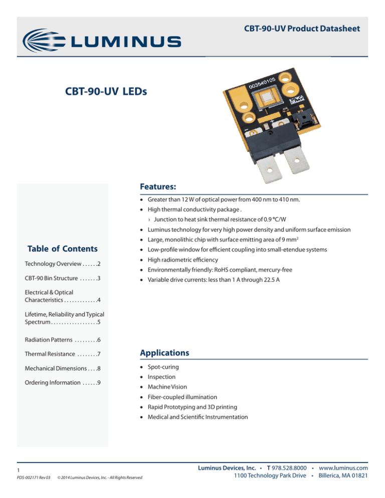
CBT-90-UV Product Datasheet CBT-120 Product Preliminary CBT-90-UV LEDs Features: •• Greater than 12 W of optical power from 400 nm to 410 nm. •• High thermal conductivity package . ›› Junction to heat sink thermal resistance of 0.9 °C/W •• Luminus technology for very high power density and uniform surface emission Table of Contents Technology Overview. . . . . . 2 CBT-90 Bin Structure . . . . . . . 3 •• Large, monolithic chip with surface emitting area of 9 mm2 •• Low-profile window for efficient coupling into small-etendue systems •• High radiometric efficiency •• Environmentally friendly: RoHS compliant, mercury-free •• Variable drive currents: less than 1 A through 22.5 A Electrical & Optical Characteristics. . . . . . . . . . . . . 4 Lifetime, Reliability and Typical Spectrum. . . . . . . . . . . . . . . . . . 5 Radiation Patterns . . . . . . . . . 6 Thermal Resistance . . . . . . . . 7 Applications Mechanical Dimensions. . . . 8 •• Spot-curing Ordering Information . . . . . . 9 •• Inspection •• Machine Vision •• Fiber-coupled illumination •• Rapid Prototyping and 3D printing •• Medical and Scientific Instrumentation 1 PDS-002171 Rev 03 © 2014 Luminus Devices, Inc. - All Rights Reserved Luminus Devices, Inc. • T 978.528.8000 • www.luminus.com 1100 Technology Park Drive • Billerica, MA 01821 CBT-90-UV Product Datasheet Technology Overview Luminus Big Chip LEDs™ benefit from innovations in device technology, chip packaging and thermal management. This suite of technologies give engineers and system designers the freedom to develop solutions both high in power and efficiency. Luminus Technology Reliability Luminus’ technology enables large area LED chips to emit photons uniformly over the entire LED chip surface. The intense optical power density produced by these UV LEDs™ facilitate designs which replace arc and halogen lamps where arrays of traditional high power LEDs cannot. For UV devices, Luminus engineers the LEDs™ to maximize light extraction and to emit with a Lambertian far-field distribution pattern. The design maximizes efficiency and allows for flexible optical designs. Designed from the ground up, Luminus LEDs are one of the most reliable light sources in the world today. Big Chip LEDs have passed a rigorous suite of environmental and mechanical stress tests, including mechanical shock, vibration, temperature cycling and humidity, and have been fully qualified for use in extreme high power and high current applications. With very low failure rates and median lifetimes that typically exceed 10,000 hours, Luminus Big Chip LEDs are ready for even the most demanding applications. Packaging Technology Environmental Benefits Thermal management is critical in high power LED applications. With a thermal resistance from junction to heat sink of 0.9°C/W, Luminus CBT-90-UV LEDs have the lowest thermal resistance of any LED on the market. This allows the LED to be driven at higher current densities while maintaining a low junction temperature, thereby resulting in brighter solutions and longer lifetimes. Luminus LEDs help reduce power consumption and the amount of hazardous waste entering the environment. All LED products manufactured by Luminus are RoHS compliant and free of hazardous materials, including lead and mercury. Understanding Big Chip LED Test Specifications Every Luminus LED is fully tested to ensure that it meets the high quality standards expected from Luminus’ products. Testing Temperature Multiple Operating Points Luminus core board products are typically measured in such a way that the characteristics reported agree with how the devices will actually perform when incorporated into a system. This measurement is accomplished by mounting the devices on a 40ºC heat sink and measuring the device while fully powered. The tables on the following pages provide typical optical and electrical characteristics. Since the LEDs can be operated over a wide range of drive conditions(currents from <1A to 22.5 A, and duty cycle from <1% to 100%), multiple drive conditions maybe listed. This method of measurement ensures that Luminus Big Chip LEDs perform in the field just as they are specified. CBT-90-UV devices are production specified at 13.5 A. Driving devices beyond recommended driving conditions shortens lifetime (see derating curves on page 6). 2 PDS-002171 Rev 03 © 2014 Luminus Devices, Inc. - All Rights Reserved Luminus Devices, Inc. • T 978.528.8000 • www.luminus.com 1100 Technology Park Drive • Billerica, MA 01821 CBT-90-UV Product Datasheet CBT-120 Product Datasheet CBT-90-UV Bin Structure CBT-90 LEDs are specified for Radiant Flux (power) and wavelength at a drive current of13.5 A (1.5 A/mm2) and placed into one of the following luminous flux (F) and wavelength (123) bins: Power Bins Color Power Flux Bin (F) Minimum Flux (W) Maximum Flux (W) L 12.1 13.3 M 13.3 14.6 Wavelength Bin (123) Minimum Wavelength (nm) Maximum Wavelength (nm) 400 400 405 405 405 410 UV *Note: Luminus maintains a +/- 6% tolerance on power measurements. Wavelength Bins Color UV For ordering information, please refer to page 5 of CBT-90-UV Binning & Labeling Document PDS-002172. 3 PDS-002171 Rev 03 © 2014 Luminus Devices, Inc. - All Rights Reserved Luminus Devices, Inc. • T 978.528.8000 • www.luminus.com 1100 Technology Park Drive • Billerica, MA 01821 CBT-90-UV Product Datasheet CBT-120 Product Datasheet Reference Optical & Electrical Characteristics (Ths = 40°C)1,2 UV Drive Condition 9A Parameter Symbol Current Density 13.5 A Values3 Unit J 1.0 1.5 A/mm2 VF min - 3.2 V VF 3.3 3.4 V VF max - 4.0 V Radiometric Flux Φtyp 8.9 13.4 W Radiometric Flux Density ΦR 0.55 0.83 W/mm2 Wavelength Range λ 400 - 410 400 - 410 nm Peak Wavelength λp 405 405 nm Δλ1/2 14 14 nm Forward Voltage 4 FWHM Symbol Emitting Area Emitting Area Dimensions Dynamic Resistance UV Unit 9 mm2 3 × 3 mm × mm Ωdyn 0.02 ­Ω Symbol UV Unit 22.5 A 150 °C -40 to +100 ­°C Absolute Maximum Ratings Maximum Current 5 Maximum Junction Temperature 6 Storage Temperature Range Tjmax Note 1: Data verified with NIST calibration standard. Note 2: All data are based on test conditions with a constant heat sink temperature Ths = 40°C under pulse testing conditions. Listed drive conditions are typical for common applications. CBT-90-UV devices can be driven at currents ranging from <1 A to 22.5 A and at duty cycles ranging from 1% to 100%. Drive current and duty cycle should be adjusted as necessary to maintain the junction temperature desired to meet application lifetime requirements. See Thermal Resistance section for Tj and Ths definition. Note 3: Unless otherwise noted, values listed are typical. Devices are production tested and specified at 13.5 A. Note 4: Total flux from emitting area at listed peak wavelength. Reported performance is included to show trends for a selected power level. For product roadmap and future performance of devices, contact Luminus. Note 5: CBT-90-UV LEDs are designed for operation to an absolute maximum current as specified above. Product lifetime data is specified at recommended forward drive currents. Sustained operation at or beyond absolute maximum currents will result in a reduction of device life time compared to recommended forward drive currents. Actual device lifetimes will also depend on junction temperature. Refer to the lifetime derating curves for further information. In pulsed operation, rise time from 10-90% of forward current should be longer than 0.5 μseconds. Note 6: Lifetime dependent on LED junction temperature. Input power and thermal system must be properly managed to ensure lifetime. See charts on page 6 for further information. Note 7: Special design considerations must be observed for operation under 1 A. Please contact Luminus for further information. 4 PDS-002171 Rev 03 © 2014 Luminus Devices, Inc. - All Rights Reserved Luminus Devices, Inc. • T 978.528.8000 • www.luminus.com 1100 Technology Park Drive • Billerica, MA 01821 CBT-90-UV Product Datasheet CBT-120 Product Datasheet Optical Power Characteristics Relative Power vs Forward Current (If) Normalized to 13.5 A Relative Power vs Junction Temperature (Tj) Normalized to 80°C 1.1 1.8 1.6 1.05 1.2 Relative Power Relative Power 1.4 1 0.8 0.6 0.4 1 0.95 0.9 0.2 0 0.85 0 5 10 15 20 40 25 50 60 If - Forward Current [Amps] 70 80 90 100 110 120 110 120 110 120 Tj - Junction Temperature [°C] Forward Voltage Characteristics Change in Forward Voltage (Vf) vs Junction Temperature (Tj) Referenced to 80°C Change in Forward Voltage (Vf) vs Forward Current (If) Referenced to 13.5 A 0.12 Change in Forward Voltage [Volts] Change in Forward Voltage [Volts] 0.4 0.2 0 -0.2 -0.4 -0.6 0.1 0.08 0.06 0.04 0.02 0 -0.02 -0.04 -0.06 -0.08 -0.1 -0.8 0 5 10 15 20 40 25 50 60 70 80 90 100 Tj - Junction Temperature [°C] If - Forward Current [Amps] Peak Wavelength Characteristics Change in Peak Wavelength (λp) vs Forward Current (If) Referenced to 13.5 A Change in Peak Wavelength (λp) vs Temperature (Tj) Referenced to 80°C 2.5 Change in Peak Wavelength [nm] Change in Peak Wavelength [nm] 1.5 1 0.5 0 -0.5 -1 -1.5 2 1.5 1 0.5 0 -0.5 -1 -1.5 -2 -2.5 0 5 10 15 If - Forward Current [Amps] 5 PDS-002171 Rev 03 © 2014 Luminus Devices, Inc. - All Rights Reserved 20 25 40 50 60 70 80 90 100 Tj - Junction Temperature [°C] Luminus Devices, Inc. • T 978.528.8000 • www.luminus.com 1100 Technology Park Drive • Billerica, MA 01821 CBT-90-UV-415 Product Datasheet CBT-90-UV Product Datasheet Preliminary CBT-90-UV B50 Reliability8 CBT90-UV-405 nm Derating Curve B50 Lifetime (Median of Population) 40kh 35kh 13 B50 Lifetime (Hours) IF-Maximum Current (A) 15 CBT90-UV-405 nm B50 Projected Lifetime 11 B50 ≥ 10kh 9 B50 ≥ 15kh 7 B50 ≥ 20kh 90 25kh 20kh 15kh 10kh 5kh 5 80 30kh 100 110 120 130 140 Maximum Junction Temperature (°C) 150 160 0 90 100 110 120 130 Junction Temperature (°C) 140 150 CBT-90-UV B10 Reliability8 CBT90-UV-405 nm Derating Curve B10 Lifetime (10% of Population) 40kh B10 Lifetime (Hours) IF-Maximum Current (A) 15 13 11 9 B10 ≥ 10kh 7 B10 ≥ 15kh 90 35kh 30kh 25kh 20kh 15kh 10kh 5kh B10 ≥ 20kh 5 80 CBT90-UV-405 nm B10 Projected Lifetime 100 110 120 130 140 Maximum Junction Temperature (°C) 150 160 0 80 Typical Spectrum 90 100 110 120 130 Junction Temperature (°C) 140 150 Relative Power 1 0.8 0.6 Full-Width Half-Maximum 0.4 0.2 0 380 400 420 Wavelength (nm) 440 Note 8 Lifetime defined as time to 70% of initial intensity. Based on preliminary lifetime test data. Data can be used to model failure rate over typical product lifetime. 6 PDS-002171 Rev 03 © 2014 Luminus Devices, Inc. - All Rights Reserved Luminus Devices, Inc. • T 978.528.8000 • www.luminus.com 1100 Technology Park Drive • Billerica, MA 01821 CBT-90-UV Product Datasheet CBT-120 Product Datasheet Typical Radiation Pattern 120% Violet cosine function Normalized Intensity 100% 80% 60% 40% 20% 0% -90 -75 -60 -45 -30 -15 0 15 Angle [degrees] 30 45 60 75 90 Thermal Resistance Typical Thermal Resistance Window Frame Thermistor, Tref Window Die Junction, Tj Copper Core-Board, Tb Thermal Interface Material Heatsink (3 mm from core-board), Ths Rθj-b1 0.80 °C/W Rθb-hs1 0.12 °C/W Rθj-hs2 0.92 °C/W Rθj-ref1 0.83 °C/W Note 1: Thermal resistance values are based on FEA model results correlated to measured Rθj-hs data. Note 2: Thermal Resistance is based on eGraf 1205 Thermal interface. Ambient, Ta Thermistor Information Electrical Pinout The thermistor used in CBT-90 devices mounted on coreboards is from Murata Manufacturing Co. The global part number is NCP18XH103J03RB. Please see http://www.murata.com/ for details on calculating thermistor temperature. For more information on use of the thermistor, please contact Luminus directly. 7 PDS-002171 Rev 03 © 2014 Luminus Devices, Inc. - All Rights Reserved 1 2 Luminus Devices, Inc. • T 978.528.8000 • www.luminus.com 1100 Technology Park Drive • Billerica, MA 01821 CBT-90-UV Product Datasheet CBT-120 Product Datasheet Mechanical Dimensions – CBT-90-UV Emitter ',0(16,216,10,//,0(7(56 ; ',((0,77,1* $5($ ( ' ',((0,77,1* $5($ ; $ % & ( 6(&7,21(( ; '(7$,/' ',0(16,21 1$0( '(6&5,37,21 120,1$/ ',0(16,21 $ 7232)0(7$/68%675$7(727232):,1'2: % 7232)',((0,77,1*$5($727232):,1'2: & 7232)0(7$/68%675$7(727232)',((0,77,1*$5($ 72/(5$1&( ':* Recommended connector for Anode and Cathode: Panduit Disco Lok™ Series P/N: DNG14-250FL-C. Thermistor Connector: MOLEX P/N 53780-0270. Recommended Female: MOLEX P/N 51146-0200 or equivalent. 8 PDS-002171 Rev 03 © 2014 Luminus Devices, Inc. - All Rights Reserved Luminus Devices, Inc. • T 978.528.8000 • www.luminus.com 1100 Technology Park Drive • Billerica, MA 01821 CBT-90-UV Product Datasheet Ordering Information Products Ordering Part Number CBT-90-UV-C31 CBT-90-UV-C31-x123-22 Description CBT-90 -UV consisting of a 9 mm2 LED, a thermistor, connectors, and a copper-core PCB. Note: For information on ordering specific bins or bin ranges please refer to the CBT-90-UV Binning and Labeling document PDS-002172. ULTRAVIOLET RADIATION Avoid eye and skin exposure The products, their specifications and other information appearing in this document are subject to change by Luminus Devices without notice. Luminus Devices assumes no liability for errors that may appear in this document, and no liability otherwise arising from the application or use of the product or information contained herein. None of the information provided herein should be considered to be a representation of the fitness or suitability of the product for any particular application or as any other form of warranty. Luminus Devices’ product warranties are limited to only such warranties as accompany a purchase contract or purchase order for such products. Nothing herein is to be construed as constituting an additional warranty. No information contained in this publication may be considered as a waiver by Luminus Devices of any intellectual property rights that Luminus Devices may have in such information. Big Chip LEDs™ is a registered trademark of Luminus Devices, Inc., all rights reserved. This product is protected by U.S. Patents 6,831,302; 7,074,631; 7,083,993; 7,084,434; 7,098,589; 7,105,861; 7,138,666; 7,166,870; 7,166,871; 7,170,100; 7,196,354; 7,211,831; 7,262,550; 7,274,043; 7,301,271; 7,341,880; 7,344,903; 7,345,416; 7,348,603; 7,388,233; 7,391,059 Patents Pending in the U.S. and other countries. 9 PDS-002171 Rev 03 © 2014 Luminus Devices, Inc. - All Rights Reserved Luminus Devices, Inc. • T 978.528.8000 • www.luminus.com 1100 Technology Park Drive • Billerica, MA 01821
