Phase-Locked Loops with Applications
Phase-Locked Loops with
Applications
ECE 5675/4675 Lecture Notes
Spring 2011
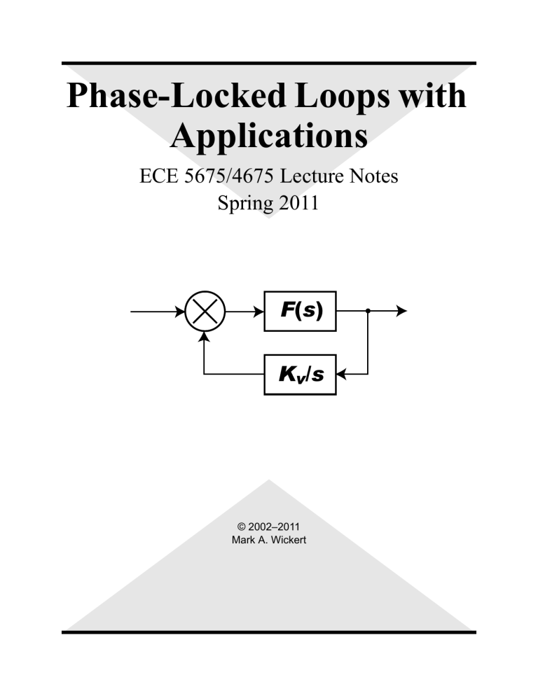
F ( s )
K v
/ s
© 2002–2011
Mark A. Wickert
.
Chapter
1
Course Introduction/Overview
Contents
1.1 Lecture Outline . . . . . . . . . . . . . . . . . . . . . 1-3
1.2 This Course and the Phase-Locked Loop Landscape . 1-4
1.2.1 General PLL Perspective . . . . . . . . . . . . .
1-4
1.2.2 Course Topics . . . . . . . . . . . . . . . . . . .
1-5
1.3 Course Perspective in the Comm/DSP Area of ECE . 1-7
1.4 Computer Analysis/Simulation Tools . . . . . . . . . . 1-8
1.5 Instructor Policies . . . . . . . . . . . . . . . . . . . . 1-9
1.6 Course Syllabus . . . . . . . . . . . . . . . . . . . . . 1-10
1.7 Required Student Background . . . . . . . . . . . . . 1-11
1.8 References . . . . . . . . . . . . . . . . . . . . . . . . 1-12
1.9 PLL Introduction . . . . . . . . . . . . . . . . . . . . 1-14
1.9.1 Classification of PLLs . . . . . . . . . . . . . . 1-14
1.9.2 LPLL . . . . . . . . . . . . . . . . . . . . . . . 1-15
1.9.3 DPLL . . . . . . . . . . . . . . . . . . . . . . . 1-16
1.9.4 ADPLL . . . . . . . . . . . . . . . . . . . . . . 1-17
1.9.5 SPLL . . . . . . . . . . . . . . . . . . . . . . . 1-18
1.10 Applications Overview . . . . . . . . . . . . . . . . . 1-20
1-1
CHAPTER 1. COURSE INTRODUCTION/OVERVIEW
1.10.1 Synchronization for Digital Communications . . 1-20
1.10.2 Frequency Synthesis Applications . . . . . . . . 1-27
1.11 Simulation Examples . . . . . . . . . . . . . . . . . . 1-30
1-2 ECE 5675 Phase-Lock Loops with Applications
1.1. LECTURE OUTLINE
1.1 Lecture Outline
� This Course and the PLL Landscape
– General PLL perspective
– Course Topics
� Course perspective in the comm/DSP area of ECE
� The role of computer analysis/simulation tools
� Instructor policies
� Course syllabus
� Required student background
� References
– Books
– Reports
– Journals
� PLL introduction and applications overview
ECE 5675 Phase-Lock Loops with Applications 1-3
CHAPTER 1. COURSE INTRODUCTION/OVERVIEW
1.2 This Course and the Phase-Locked
Loop Landscape
1.2.1 General PLL Perspective
� The focus of this course is phase-lock loops (PLLs) and applications
� At first this may seem like a very narrow course of study, but the PLL has many applications and many implementation variations
� The use of PLLs for frequency synthesis, i.e., creating a stable yet tuneable local oscillator for radio transmitters and receivers is one traditional application area
� In communication systems in general the PLL is widely used
– Carrier phase and frequency tracking
– Symbol (bit) synchronization
– Chip synchronization is spread-spectrum systems (this includes GPS receivers)
� Clock recovery (same class of problems as symbol sync)
� The implementation may be:
– All analog electronics (microwave/RF/baseband)
– A hybrid of analog and digital electronics
– A hybrid of analog and software
– Pure software
1-4 ECE 5675 Phase-Lock Loops with Applications
1.2. THIS COURSE AND THE PHASE-LOCKED LOOP LANDSCAPE
� The implementation technology may be:
– Board level using RF and baseband devices
– Single chip with a few off-chip or maybe no off-chip parts
– Custom ASIC or FPGA
– A combination of RF and baseband analog with the remainder in software via a real-time digital signal processing
– Entirely real-time DSP approach if signal samples are acquired somewhere else
1.2.2 Course Topics
� PLL fundamentals
– Loop components
– Loop response
– Loop stability
– Transient response
– Modulation response
� Digital PLLs
� Performance in noise
– Input noise
– Phase noise
– Nonlinear behavior and cycle slipping
ECE 5675 Phase-Lock Loops with Applications 1-5
CHAPTER 1. COURSE INTRODUCTION/OVERVIEW
� Acquisition
– Unaided
– Aided
� Analog PLL lab experiment
� Communication applications
– DSP-based carrier phase tracking algorithms
– DSP-based symbol timing tracking algorithms
1-6 ECE 5675 Phase-Lock Loops with Applications
1.3. COURSE PERSPECTIVE IN THE COMM/DSP AREA OF ECE
1.3 Course Perspective in the Comm/DSP
Area of ECE
Signal Process
Signal Process
ECE 5675 Phase-Lock Loops with Applications 1-7
CHAPTER 1. COURSE INTRODUCTION/OVERVIEW
1.4 Computer Analysis/Simulation Tools
� In working homework problems pencil and paper type solutions will work for most problems
� Often times solutions can be enhanced through the use of computer analysis and simulation tools
� At least one computer project will be assigned which involves both mathematical modeling and simulation
� Most often MATLAB will suffice for modeling and simulation
� The use of Spice with behavioral level modeling capabilities may also be useful, e.g., XSpice via SIMetrix/SIMPLIS or
PSpice
� Block level simulation environments are particularly convenient for PLL simulations
– MATLAB Simulink: very powerful block simulation environment, most capable for PLL work when expanded with DSP blockset and the Comm block set; limited PLL specific blocks even in Comm block set
– VisSim/Comm (included with the student version of Mathcad: A friendly block simulation environment, which with the Comm library is very good at complex baseband simulation; PLL components are also included
– Elanix SystemView (used the last time the course was taught): free student version which has a RF and Comm block set with some PLL specific oriented blocks
1-8 ECE 5675 Phase-Lock Loops with Applications
1.5. INSTRUCTOR POLICIES
1.5 Instructor Policies
� Working homework problems will be a very important aspect of this course
� Each student is to his/her own work and be diligent in keeping up with problem assignments
� If work travel keeps you from attending class on some evening, please inform me ahead of time so I can plan accordingly, and you can make arrangements for turning in papers
� The course web site http://www.eas.uccs.edu/wickert/ece5675/ will serve as an information source in between weekly class meetings
� Please check the web site updated course notes, assignments, hints pages, and other important course news
ECE 5675 Phase-Lock Loops with Applications 1-9
CHAPTER 1. COURSE INTRODUCTION/OVERVIEW
1.6 Course Syllabus
ECE 5675/4675 Phase-Locked Loops,
Synchronization, and Frequency Synthesis
Spring Semester 2011
!"#$%&'$(%) Dr. Mark Wickert *++,'-) EB-226 wickert@eas.uccs.edu
http://www.eas.uccs.edu/wickert/ece5675
./("-)
012)
262-3500
262-3589
*++,'-34%#) Tue. 3:30 pm–4:15 pm and after 7:05 pm as needed, others by appointment.
Note: These hours may be adjusted if needed.
5-6&,%-73
8-2$#)
F. M. Gardner, Phaselock Techniques , third edition, John Wiley, New York,
2005. (ISBN: 0-471-43063-3)
*9$,("1:3
8-2$)
*9$,("1:3
;(+$<1%-)
M. Rice, Digital Communications A Discrete-Time Approach, Prentice Hall,
New Jersey, 2009. (ISBN 978-0-13-030497-1)
MATLAB Student Version 7.x, Simulink 5.x, and Symbolic Math Toolbox
Available for Windows/Linux/Mac OSX. The signal processing and control toolboxes, Simulink, and DSP block set are now included with the student version. Note: The ECE PC Lab has the full version of MATLAB and Simulink for windows (ver. 7.x) with many toolboxes. Other tools of interest include
VisSim/Comm ( !!!"#$%%$&"'(&) ), Mathematica 7 (see course Web Site about how to download).
=%17,">) 1.) Graded homework assignments totaling 40%.
2.) Mid-term Exam worth 25%.
3.) Analog PLL Laboratory 10%.
4.) Final Project/Exam worth 25%.
8(9,'# 8-2$3?/19$-%#
;-##,("3
@<A#B
1. Introduction/Overview
2. Phase-Locked Loop Fundamentals (including basic synthesizers)
3. Digital Signal Processing Based PLLs
4. PLL Tracking Performance in Noise (including phase noise)
5. Unaided and Aided Acquisition
6. Anomalous Locking*
7. Analog PLL Lab Experiment
8. PLL Frequency Synthesizers*
9. Real-time DSP PLL Experiment*
10. Synchronization techniques in Digital Comm Systems*
1
2, 3, 5, 10, 11, 12,
15, 16, Rice App C
4, 13, Rice App C
6, 7, 9, 10
8
14
Handout
15
Handout
Notes, 17, Rice 7 & 8
1.0
3.0
2.0
2.0
1.0
0.5
2.0
1.0
1.0
2.0
Requirements : A background in basic communication theory, probability and random variables, and basic digital signal processing, i.e. sampling theory would be desired. Please contact Dr. Wickert if you are considering this course, but are in doubt as to whether you have adequate background. Items with * will be selected by class interest.
1-10 ECE 5675 Phase-Lock Loops with Applications
1.7. REQUIRED STUDENT BACKGROUND
1.7 Required Student Background
� Basic linear systems theory is a must
� Random variables is needed for noise analysis
– A brief introduction to random processes will be provided if needed
� Basic modulation theory is also assumed
� A knowledge of digital communication systems is desirable
� A basic understanding of digital signal processing would be helpful, but is not required
� Knowledge of sampling theory is needed for digital loop concepts
� Knowledge of z -domain concepts is desirable, but again a brief introduction will be given if needed
� The ability to program using MATLAB is important for simulation aspects
� The ability to build Spice circuit models is also desirable
ECE 5675 Phase-Lock Loops with Applications 1-11
CHAPTER 1. COURSE INTRODUCTION/OVERVIEW
1.8 References
The following list of references is not exhaustive by any means, but is a list core of books I have in my library or have been recommended to me. Some of these books are hard to find since they are now outof-print.
General PLL
1. Heinrich Meyr and Gerd Ascheid, Synchronization in Digital Communications , Volume 1, John Wiley, 1990.
� This text is basically concerned with analog PLLs (including chargepump) starting from the very basic concepts all the way through very detailed nonlinear analysis with noise
� The text also includes material on automatic frequency control (AFC) and automatic gain control (AGC)
� The book is clearly telecommunications based since PLL synthesizers are not considered at all
� Used as the course text in earlier (1990’s offering’s of the course)
2. Alain Blanchard, Phase-Locked Loops: Application to Coherent Receiver
Design , Wiley, New York,1976. Original course text Dr. Wickert used in his first PLL course.
3. William F. Egan, Phase-Lock Basics , second edition, John Wiley, 2008.
First edition used in 2004 offering of the course.
4. Roland E. Best, Phase-Locked Loops, Theory Design, and Applications , fifth edition, McGraw Hill, 2003.
5. Dan Wolaver, Phase-Locked Loop Circuit Design , Prentice Hall, New Jersey, 1991.
6. James A. Crawford, Advanced Phase-Lock Techniques , Artech House, Boston,
MA, 2008.
7. Jack K. Holmes, Coherent Spread Spectrum Systems , John Wiley, 1982.
1-12 ECE 5675 Phase-Lock Loops with Applications
1.8. REFERENCES
8. Jacob Klapper and John T. Frankle, Phase-Locked and Frequency-Feedback
Systems , Academic Press, New York, 1972.
9. William C. Lindsey and Marvin K. Simon, Telecommunication Systems Engineering , Prentice-Hall, Englewood Cliffs, New Jersey, 1973.
10. A. J. Viterbi, Principles of Coherent Communications , McGraw-Hill, New
York, 1966.
11. Rodger E. Ziemer and Roger L. Peterson, Digital Communications and
Spread Spectrum Systems , Macmillan, New York, 1985.
Frequency Synthesizers
1. William F. Egan, Frequency Synthesis by Phase Lock , second edition, Wiley, New York, 2000.
2. Venceslav F. Kroupa, Frequency Synthesis: Theory, Design, and Applications , Wiley, New York, 1973.
3. Vadim Manassewitsch, Frequency Synthesizers: Theory and Design , 3rd ed., Wiley, New York, 1987.
4. W. P. Robbins, Phase Noise in Signal Sources (Theory and Applications) ,
Peter Peregrinus Ltd., London, UK., 1982.
5. Ronald C. Stirling, Microwave Frequency Synthesizers , Prentice-Hall, Englewood Cliffs, New Jersey, 1987.
Synchronization
1. Umberto Mengali and Aldo N. D’Andrea, Synchronization Techniques for
Digital Receivers , Plenum Press, New York, 1997.
2. Heinrich Meyr, Marc Moeneclaey, and Stefan Fechtel, Digital Communication Receivers: Synchronization, Channel Estimation, and Signal Processing , Prentice Hall, New Jersey, 1998. This is volume II of of Meyr and
Ascheid.
Reports
1. L. Bogusch, “Digital Communications in Fading Channels: Tracking and
Synchronization,” AFWL-TR-90-15, Weapons Laboratory, Kirkland AFB,
NM, 1990.
ECE 5675 Phase-Lock Loops with Applications 1-13
CHAPTER 1. COURSE INTRODUCTION/OVERVIEW
Journals
1. IEEE Transactions on Communications.
2. IEEE Journal on Select Areas in Communications.
1.9 PLL Introduction
The history of the phase-locked loop dates back to as early as 1932.
According to author Dr. Rolland Best, the French engineer de Bellesize is the inventor of coherent communication. Current applications of the phase-locked loop (PLL) in-clude more than just coherent communications. Frequency synthesis is currently a very important
PLL application area. The emphasis of this course will however be for the most part on basic PLL theory and telecommunication applications. A discussion of various synthesizer types will also be included at some point.
1.9.1 Classification of PLLs
In this course the intention is to discuss four basic classes of PLLs.
Using the notation of Best 1 these classes are:
� Analog or Linear PLL (LPLL)
� Digital PLL (DPLL)
� All digital PLL (ADPLL)
� Software PLL (SPLL)
1 Roland E. Best, Phase Locked-Loops: Theory, Design, and Applications, fourth edition, Mc-
Graw Hill, 1999
1-14 ECE 5675 Phase-Lock Loops with Applications
1.9. PLL INTRODUCTION
1.9.2 LPLL
The LPLL (Best) or analog PLL is the classical form of PLL. All components in the LPLL operate in the continuous-time domain. A
LPLL block diagram is shown below:
� The phase detector is typically some form of analog multiplier, either a double-balanced mixed (DBM) or an active fourquadrant multiplier
� The phase error function is of the form
�.t / D K m
K
1
A
K
D sin
�
�.t / � O � .t /
�
� K
D
�
�.t / � O � .t /
�
2 A sin
[ ω
0 t +
θ t
]
2 A cos
[ ω
0 t +
θ ]
Classical analog PLL
� The loop filter may be active or passive, but it typically results in the loop being either first-order or second-order
� The design/analysis of the loop filter makes use of the Laplace transform
ECE 5675 Phase-Lock Loops with Applications 1-15
CHAPTER 1. COURSE INTRODUCTION/OVERVIEW
� Loop filter system functions, F .s/ , include:
Loop Order
1
2(perfect integrator)
2(imperfect integrator)
2(lag or lowpass)
Filter F .s/
1
1 C s�
2 s�
1
1 C s�
2
1 C s�
1
1
1 C s�
1.9.3 DPLL
The digital PLL is really just an analog PLL with a digital phase detector.
� The DPLL is really a hybrid system
� The DPLL is very popular in synthesizer applications
� In the above figure the optional digital divider, and variations on it, are used in frequency synthesis applications
1-16
� Popular types of digital phase detectors include:
– Exclusive or gate (EXOR)
– Edge-triggered JK-flipflop
– Phase frequency detector (PFD)
ECE 5675 Phase-Lock Loops with Applications
2 A sin
[ ω
0 t +
θ t
]
1.9. PLL INTRODUCTION
2 A cos
[
N
ω
0 t + N
θ ]
2 A cos
[ ω
0 t +
θ ]
Classical digital PLL (digital phase detector)
1.9.4 ADPLL
The all-digital PLL (classical all-digital) is distinctly different from the first two PLLs mentioned thus far.
� The ADPLL is a digital loop in two senses:
– All digital components
– All digital (discrete-time) signals
� There are many ADPLL building blocks, and many variations on putting them together
– The ADPLL is also closely related to the SPLL
� The VCO is replaced by a digitally controlled oscillator (DCO) or also called a numerically controlled oscillator (NCO)
ECE 5675 Phase-Lock Loops with Applications 1-17
CHAPTER 1. COURSE INTRODUCTION/OVERVIEW
All-digital PLL as implemented in the part 74xx297
1.9.5 SPLL
The SPLL can be viewed as a discrete-time implementation of either the LPLL or the DPLL. The block diagram of a generic SPLL is shown below.
1-18
� The implementation of the loop filter is typically a difference equation
� The design/analysis of the loop filter is done using the z-transform
ECE 5675 Phase-Lock Loops with Applications
1.9. PLL INTRODUCTION
� The SPLL is feasible due to the availability of digital signal processing (DSP) oriented microprocessors
– A DSP processor features a Harvard architecture (separate data and program memories)
– Pipelined instruction capabilities
� The computer hardware requirements are relatively high, but the flexibility is also very great
� By designing the SPLL to closely match say an LPLL we can effectively simulate analog PLL designs using software tools
2 A sin
( ω
0 t +
θ t
)
f s
2 A cos
( ω
0 t +
θ )
A software or discrete-time signals based PLL
� The SPLL is very popular in digital communication applications
� For complex baseband systems a popular phase detector is again the sinusoidal phase detector, but now it takes the following form
ECE 5675 Phase-Lock Loops with Applications 1-19
CHAPTER 1. COURSE INTRODUCTION/OVERVIEW
K
1
Ae
– j
( θ n –
ˆ )
Ae j
( ω
0 n +
θ n
)
K
1 e
– j
( ω
0 n +
θ )
K
1
A sin
( θ n –
ˆ )
Complex signal form of SPLL
1.10 Applications Overview
1.10.1 Synchronization for Digital Communications
� In digital communications various levels of synchronization are required
� Systems that only operate at baseband typically require fewer total function than those at passband or RF
� The synchronization problem can viewed as one of parameter estimation from waveforms
� The three parameters most often referred to are, carrier frequency, f
0
, carrier phase,
�
, and symbol timing,
�
1-20
� Taken jointly they form a parameter vector with three components
ECE 5675 Phase-Lock Loops with Applications
1.10. APPLICATIONS OVERVIEW
e
– j 2
π v t
r
′ t e
– j
θ
x t
[ ]
kT +
τ
c ˆ k
Synchronization in digital communications using complex signals
� The figure above depicts analog signal processing, but in practice combinations of analog and digital signal processing are required
� Parameter tracking can be implemented using feedback, as in
PLL based techniques
� Feed-forward methods are also possible
� Some block diagrams of synchronization systems are shown next
Coherent Carrier Reference Generation
( ) 2
ECE 5675 Phase-Lock Loops with Applications
1-21
CHAPTER 1. COURSE INTRODUCTION/OVERVIEW
Squaring loop for suppressed carrier modulation
90
°
Costas loop which performs at baseband the operation of the squaring loop
( ) M
M th-power loops for
M
-ary phase shift keying
A DSP Based
M th Power and Decision Directed Approach
1-22
� In bandpass digital communication systems the carrier frequency is generated from a local timing reference
ECE 5675 Phase-Lock Loops with Applications
1.10. APPLICATIONS OVERVIEW
� At the receiver coherent demodulation requires that the same carrier frequency (or a translated version) and phase be used for demodulation
� A coherent carrier recovery system, which tracks the frequency and phase of the carrier at the receiver, is used for this purpose
� The received signal (noiseless) is of the form x.t / D Re
˚ s.t /e j Œ!
c t C �.t /�
�
� Consider a complex baseband information carrying waveform given by (here pulse amplitude modulation PAM) y.t / D e j Œ!
c t C �.t /� m D�1
A m p.t
� mT / where A m is the data, p.t / is the transmit pulse shape, T is the symbol period, and q.t / is the frequency offset and phase jitter
� We need to form an estimate of the received carrier phase q.t / so that the above signal can be demodulated with e
� j Œ!
c t C O
� In a digital (DSP) based receiver we may sample the signal at the symbol rate (or a submultiple), the product of the carrier estimate with the input to obtain yŒn� D e j Œ�.nT / � O m D�1
A m p.nT
� mT /
ECE 5675 Phase-Lock Loops with Applications 1-23
CHAPTER 1. COURSE INTRODUCTION/OVERVIEW
� Assuming that p.nT
� mT / D ı.n/ the samples we obtain are of the form yŒn� D e j.� Œn� � O
A n
( ) M
e
– j
( ω
0 nT +
θ )
M th Power Loop
ˆ
A n
e
– j
( ω
0 nT +
θ )
Decision Directed Loop
1-24 ECE 5675 Phase-Lock Loops with Applications
1.10. APPLICATIONS OVERVIEW
Symbol/Bit Synchronization
Nonlinear filter clock recovery using a delay and multiply circuit
T
( ) d t
+
-
T
( ) d t
Early-late gate timing recovery
ECE 5675 Phase-Lock Loops with Applications 1-25
CHAPTER 1. COURSE INTRODUCTION/OVERVIEW
( s
)
y mT s
)
y
I n
T s
=
<
T sample spacing
=
= f s symbol period
A DSP based non-synchronous clock recovery loop
Spread Spectrum Code Synchronization
+
-
1-26
Delay-lock Loop
ECE 5675 Phase-Lock Loops with Applications
1.10. APPLICATIONS OVERVIEW
1.10.2 Frequency Synthesis Applications
� In wireless applications frequency synthesizers provide local oscillators for up and down conversion of modulated signals
� Any radio based electronics that operates over multiple frequencies, likely incorporates a frequency synthesizer
� The transmitter and receiver of a cellular telephony handset is shown below
90
°
90
°
Wireless handset transmitter and receiver RF signal processing
ECE 5675 Phase-Lock Loops with Applications 1-27
CHAPTER 1. COURSE INTRODUCTION/OVERVIEW
Direct Synthesis
� Use mixing (multiplication) to build up the desired frequency and a division of a single reference frequency
– Rapid switching time is one of the features
– Bulky rf hardware (switches, mixers, filters) is a disadvantage
– Spurious frequency generation can be a big problem
Indirect Synthesis
� Indirect synthesis is another name for PLL frequency synthesis
� A basic PLL synthesizer is the following
f ref
÷
N
1 f ref
-------
N
1
f out f out
--------
N
2
÷
N
2 f out
= f ref
×
N
2
------
N
1
1-28
General indirect synthesis using a DPLL
� With indirect synthesis all by itself, large divide ratios are required to obtain fine resolution
� Being able to set the divide ratio to a fractional, non-integer value would solve this problem
ECE 5675 Phase-Lock Loops with Applications
1.10. APPLICATIONS OVERVIEW
� The basis of the fractional-N method is to alter the divide ratio
N
2 between two values
Direct Digital Synthesis (DDS)
� DDS is a DSP based method of using an N-bit accumulator to generate a phase ramp corresponding to one clock cycle
– The accumulator increments the phase by an equivalent amount of �� each clock cycle
– The output frequency is given by f out
D
N i
2 N f ref where N i corresponds to the phase step size ��
– The minimum frequency change is
�f D f ref
2 N
Δθ
θ
θ
f ref
A simple direct digital synthesis scheme
ECE 5675 Phase-Lock Loops with Applications 1-29
CHAPTER 1. COURSE INTRODUCTION/OVERVIEW
Hybrid Methods
� To meet various design goals combinations of the above method may be employed
– Several PLL synthesizers can be combined to create a multi-loop synthesizer
– DDS and a PLL can be combined to achieve fine step sizes, yet the wide tuning range of a PLL
1.11 Simulation Examples
In this section several working PLL based circuits/systems will be demonstrated using a variety of software tools. The intent is to give a flavor of what options are available in the way of simulation approaches for PLL based designs.
Example 1.1: Behavioral Level Modeling using XSpice
Analog circuit designers are well acquainted with Spice. The challenge with PLL designs is to effectively make use of behavioral modeling capabilities of modern Spice implementations. One such extension to Spice is XSpice, developed at Georgia Tech.
� We will soon learn that the full simulation of a PLL is numerically intensive because waveform fidelity at the VCO level is required, yet the bandwidth of the closed loop tracking system is much smaller than the VCO quiescent frequency
� In this example full waveform fidelity is preserved, but behavioral models, as opposed to detailed circuit models, are used for most of the loop
1-30 ECE 5675 Phase-Lock Loops with Applications
1.11. SIMULATION EXAMPLES
� The VCO quiescent frequency is chosen to be just 5000 Hz and the PLL closed-loop noise equivalent bandwidth is 100 Hz
Analog PLL (LPLL) schematic using XSpice behavioral modeling
� The input signal source and VCO are both created using a voltage controlled sinusoid generator
� The phase detector is an ideal multiplier and to remove the double frequency term following the phase detector, a transfer function behavioral level model is used
� The transfer function associated with the block AD_FREQ_LPF is H.s/ D 1000=.s
C 1000/ , a lowpass filter with cutoff frequency f c
D 1000=.2�/ D 159:15 Hz
� A loop filter of the form F .s/ D .1
C s�
2 mented in circuit form using an Op-amp
/=.s�
1
/ is imple-
� The input sinusoid is initially at 5000 Hz and the VCO quiescent frequency is also at 5000 Hz
ECE 5675 Phase-Lock Loops with Applications 1-31
CHAPTER 1. COURSE INTRODUCTION/OVERVIEW
� At 40 ms the input frequency is stepped to 5100 Hz, a 100 Hz frequency step, (the VCO gain is
K v
D 100
Hz/v)
1-32
The input sinusoid and the VCO output near t D 40 ms
� The loop breaks lock and acquires in both frequency and phaselock via the nonlinear pull-in process
� In about 70 ms the loop has settled ( t D 110 ms)
� In addition to transient or time domain modeling, Spice can be used in the AC analysis mode to characterize open and closed loop magnitude and phase response of linearized loops
� The AC analysis mode also provides for detailed noise analysis and the incorporation of phase noise models of the input source oscillator and VCO
ECE 5675 Phase-Lock Loops with Applications
1.11. SIMULATION EXAMPLES
� Ultimately closed-loop phase noise performance can be obtained using actual circuit elements mixed with behavioral level models
VCO control voltage in response to a 100 Hz frequency step at t D 40 ms
Example 1.2: Baseband PLL in XSpice
In this example high frequency modeling, e.g., the individual waveform cycles of the input and VCO are removed by abstracting to what is known as a baseband PLL model. This model will be developed in Chapter 2 of the course notes.
ECE 5675 Phase-Lock Loops with Applications 1-33
CHAPTER 1. COURSE INTRODUCTION/OVERVIEW
� The multiplier phase detector is replaced by the phase difference block followed by a nonlinearity, here a sin function
� To model a frequency step an integrator at the input converts frequency to phase with a 2� factor times a frequency deviation constant
� The VCO, which is like a frequency modulator, is modeled as an integrator with gain constant 2� � K v
D 100
Hz/v in this case
, where K v
Baseband analog PLL schematic using XSpice behavioral modeling
� A 100 Hz frequency step is applied at the input at t D 40 ms as in the previous example
� Loop transient ‘pull-in’ response is slightly different than before, but the total time required to settle is very similar
1-34 ECE 5675 Phase-Lock Loops with Applications
1.11. SIMULATION EXAMPLES
� The waveform plotted is the VCO control voltage inverted to account for the ‘+’ sign in the summer block, and then scaled by 100 to scale the waveform to instantaneous frequency deviation in Hz
VCO input in response to a 100 Hz frequency step
Example 1.3: Analog PLL Modeling in MATLAB Simulink
Spice is useful for modeling certain aspects of PLL circuits, but there are times when a complete abstraction to the system level is the most efficient means to validate a design. In this example Simulink, which is an odd-on to MATLAB (included with the student version) is used.
ECE 5675 Phase-Lock Loops with Applications 1-35
CHAPTER 1. COURSE INTRODUCTION/OVERVIEW
� The Egan text includes MATLAB m-files for complete command line nonlinear PLL simulation
� Simulink is a block diagram simulation environment, so PLL simulation here is more visual
� Simulink alone does not provide direct support for PLL’s and synchronization
– If you add to Simulink the Signal Processing toolbox, the
DSP blockset, the Communication toolbox, and finally the Communication blockset, you have some basic PLL building blocks, e.g. a VCO
– With the basic Simulink library that comes with the student version of Simulink PLL simulation requires a bit more work, but is possible
� In the example given here Simulink is used to model a bandpass analog PLL with 5 kHz center frequency and 100 Hz loop bandwidth, as in Example 1.1
Step
VCO
FM Source with f0 = 5000 Hz
Product
1000 s+1000
Transfer Fcn lpf_output
To Workspace1
7.5e-3s+1
8.836e-3s
Transfer Fcn1 vco_input
To Workspace
VCO
Voltage-Controlled
Oscillator
1-36
MATLAB Simulink model of an analog PLL at 5 kHz
ECE 5675 Phase-Lock Loops with Applications
1.11. SIMULATION EXAMPLES
� The first-order lowpass filter following the multiplier phase detector is used to remove the double frequency term at 10 kHz
� A 100 Hz frequency step is applied to the input at 40 ms
� Results very similar to the XSpice model of Example 1.1 are obtained
1.2
1
0.8
0.6
0.4
0.2
0
− 0.2
0
20 40 60
80 100 120
VCO input in response to a 100 Hz frequency step
� A small amount of noise can be seen on the VCO control signal
� This noise in reality is the double frequency term, at 10 kHz, leaking through the loop filter
� This leakage will modulate the VCO and produce annoying
FM sidebands or spurs
ECE 5675 Phase-Lock Loops with Applications 1-37
CHAPTER 1. COURSE INTRODUCTION/OVERVIEW
� This leakage is even more evident at the output of the lowpass filter
0.5
0.4
f c
= 5000 Hz
0.3
0.2
0.1
0
− 0.1
− 0.2
− 0.3
− 0.4
− 0.5
0 20 40 60
80 100 120
Phase detector lowpass filter output showing 10 kHz leakage
Example 1.4: Analog PLL Modeling in VisSim
In this example we consider the block diagram modeling tool
VisSim/Comm from Visual Solutions Inc. With the readily available
Communications library support for PLL simulation is very convenient.
1-38
� VisSim is similar to Simulink in that it is a block environment for dynamic system simulation
ECE 5675 Phase-Lock Loops with Applications
1.11. SIMULATION EXAMPLES
� With the VisSim/Comm many powerful communications blocks are available, and complete complex baseband simulation blocks are also defined
� VisSim also has an interface with MATLAB, so results can be directly imported in to MATLAB, or MATLAB can perform calculations
� Standard loop filters can be defined using loop filter blocks which directly calculate the required time constants, e.g., �
1 and
�
2 from system level specifications, e.g., loop bandwidth and damping factor
� In this first VisSim example we repeat the original XSpice example of an analog PLL at center frequency of 5000 Hz and loop bandwidth of 100 Hz
ECE 5675 Phase-Lock Loops with Applications 1-39
CHAPTER 1. COURSE INTRODUCTION/OVERVIEW
VisSim/Comm model of an analog PLL at 5 kHz
� The VCO input signal (voltage) is measured when a 100 Hz frequency step is applied at 40 ms
� The results are consistent with the previous XSpice and Simulink results
1-40
� Note also that in VisSim the block diagram and graph windows are ‘wired’ together
ECE 5675 Phase-Lock Loops with Applications
1.11. SIMULATION EXAMPLES
VCO input in response to a 100 Hz frequency step
Example 1.5: Complex Baseband PLL Modeling in VisSim
In digital signal processing based implementations, common place in digital communications, the PLL is likely top operate on complex signals, i.e., complex baseband. VisSim supports this via a complex
VCO block and other complex processing blocks. In this example a complex baseband analog PLL is constructed.
� A complex baseband PLL has the advantages of the baseband
PLL of Example 1.1, but takes complex signal inputs of the form s.t / D Ae j �2�f c t C �.t /� not phase inputs
ECE 5675 Phase-Lock Loops with Applications 1-41
CHAPTER 1. COURSE INTRODUCTION/OVERVIEW
� In this example a 2nd-order loop is constructed with center frequency at f c
D 0
(DC) having a loop bandwidth of 25 Hz
� A frequency step of 50 Hz is applied at t D 0 and both the sinusoidal phase detector output and VCO input signals are observed
� The entire VisSim simulation block diagram and plots are shown below
Complex baseband PLL with a 50 Hz frequency step input
1-42 ECE 5675 Phase-Lock Loops with Applications
1.11. SIMULATION EXAMPLES
Example 1.6: Bit Synch Modeling in VisSim
Clock recovery in baseband digital communications frequently employs a PLL. Here we assume R b
D 100 bps.
� A delay and multiply (D&M) circuit is used to generate a spectral line from the NRZ (non-return-to-zero) binary bit stream
� The power spectrum of the D&M output is also computed
Delay-and-multiply bit synch block diagram
ECE 5675 Phase-Lock Loops with Applications 1-43
CHAPTER 1. COURSE INTRODUCTION/OVERVIEW
� A 2nd-order PLL with loop bandwidth of 1 Hz is configured with the D&M output as the input signal source
� To test the acquisition and tracking of the bit synch a 1 Hz frequency step is applied as a loop disturbance
R b
= 100 bps
D&M output PSD and VCO input for a frequency step
1-44 ECE 5675 Phase-Lock Loops with Applications
1.11. SIMULATION EXAMPLES
Example 1.7: Carrier Tracking in VisSim
In this example a complex baseband implementation of carrier phase tracking is described.
� The modulation scheme is binary phase-shift keying (BPSK) with square-root raised cosine (SRC) pulse shaping
� Pulse shaping filter FIR coefficients are imported from MAT-
LAB, but could also be designed directly in the VisSim/Comm environment
� The bit rate is 10 bps and the carrier frequency is nominally 0
Hz
� To eliminate clutter a hierarchical block diagram is created
Shaped BPSK with Costas carrier phase tracking
� The modulator sub-block ( Shaped PAM ) is created to handle the pulse shaping
ECE 5675 Phase-Lock Loops with Applications 1-45
CHAPTER 1. COURSE INTRODUCTION/OVERVIEW
� The Carrier Recovery block houses a complex baseband Costas loop having a 2nd-order loop filter with loop bandwidth of 0.5
Hz
� A 0.5 Hz frequency step is applied 2 seconds into the simulation
� The carrier recovery block contains a graphical display showing how the loop acquires lock following the frequency step
Carrier recovery block showing the VCO input signal
1-46
� A matched filter having an identical SRC filter coefficients are applied to the received signal following carrier recovery
� Shown below is an eye plot at the output of this filter
� The transmitted power spectrum is also computed
ECE 5675 Phase-Lock Loops with Applications
1.11. SIMULATION EXAMPLES
Eye plot of the received BPSK and the transmit PSD
ECE 5675 Phase-Lock Loops with Applications 1-47
