Analog Applications Journal
Automotive
Reduce buck-converter EMI and voltage
stress by minimizing inductive parasitics
By Timothy Hegarty
Systems Engineer, Non-Isolated Power Solutions
Introduction
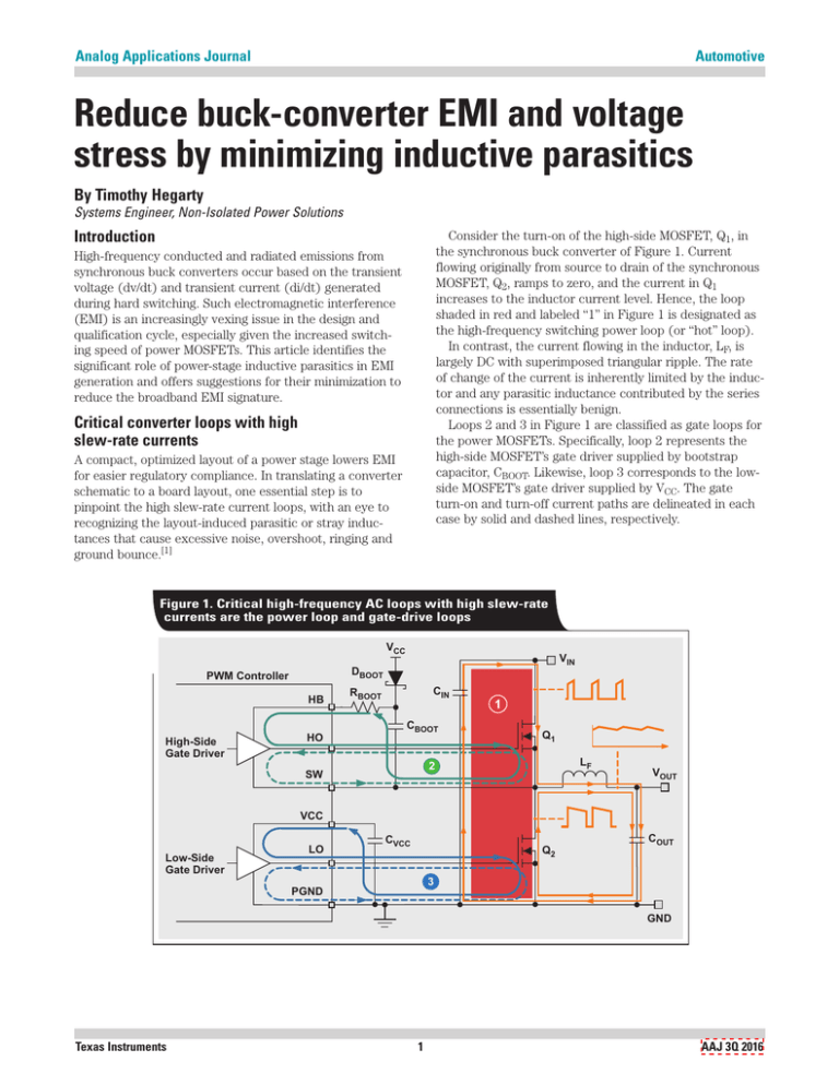
Consider the turn-on of the high-side MOSFET, Q1, in
the synchronous buck converter of Figure 1. Current
flowing originally from source to drain of the synchronous
MOSFET, Q2, ramps to zero, and the current in Q1
increases to the inductor current level. Hence, the loop
shaded in red and labeled “1” in Figure 1 is designated as
the high-frequency switching power loop (or “hot” loop).
In contrast, the current flowing in the inductor, LF, is
largely DC with superimposed triangular ripple. The rate
of change of the current is inherently limited by the inductor and any parasitic inductance contributed by the series
connections is essentially benign.
Loops 2 and 3 in Figure 1 are classified as gate loops for
the power MOSFETs. Specifically, loop 2 represents the
high-side MOSFET’s gate driver supplied by bootstrap
capacitor, CBOOT. Likewise, loop 3 corresponds to the lowside MOSFET’s gate driver supplied by VCC. The gate
turn-on and turn-off current paths are delineated in each
case by solid and dashed lines, respectively.
High-frequency conducted and radiated emissions from
synchronous buck converters occur based on the transient
voltage (dv/dt) and transient current (di/dt) generated
during hard switching. Such electromagnetic interference
(EMI) is an increasingly vexing issue in the design and
qualification cycle, especially given the increased switching speed of power MOSFETs. This article identifies the
significant role of power-stage inductive parasitics in EMI
generation and offers suggestions for their minimization to
reduce the broadband EMI signature.
Critical converter loops with high
slew-rate currents
A compact, optimized layout of a power stage lowers EMI
for easier regulatory compliance. In translating a converter
schematic to a board layout, one essential step is to
pinpoint the high slew-rate current loops, with an eye to
recognizing the layout-induced parasitic or stray inductances that cause excessive noise, overshoot, ringing and
ground bounce.[1]
Figure 1. Critical high-frequency AC loops with high slew-rate
currents are the power loop and gate-drive loops
VCC
PWM Controller
HB
High-Side
Gate Driver
VIN
DBOOT
HO
CIN
RBOOT
CBOOT
1
Q1
LF
2
SW
VOUT
VCC
Low-Side
Gate Driver
LO
CVCC
Q2
COUT
3
PGND
GND
Texas Instruments
1
AAJ 3Q 2016
Analog Applications Journal
Automotive
Parasitic inductances
expected, the power-loop inductance is highly related to
the layout geometry of the input capacitor-MOSFET loop
denoted by the red-shaded area in Figure 1.
Meanwhile, the gate-loop self-inductance, LG, includes
lumped contributions from the MOSFET package and PCB
trace routing. An inspection of Figure 2 reveals that the
common-source inductance of Q1 exists mutually in both
the power and gate loops. It increases switching loss
because the di/dt of the power loop creates a negative
feedback voltage that impedes rise and fall times of the
gate-source voltage. Another factor that leads to increased
component stress is the common-source inductance of Q2,
which contributes to spurious turn-on of the low-side
MOSFET during body-diode reverse recovery.[2]
In general, the behavior of MOSFET switching and the
consequences for waveform ringing, power dissipation,
device stress, and EMI are correlated with the parasitic
inductances of the power-loop and gate-drive circuits.
Figure 2 provides a comprehensive illustration of the parasitic elements arising from component placement, device
package, and printed circuit board (PCB) layout routing
that affect switching performance and EMI of the synchronous buck converter.
The effective high-frequency power-loop inductance,
LLOOP, is the sum of the total drain inductance, LD, and the
common-source inductance, LS, that results from the
series inductance of the input capacitor and PCB traces,
and the package inductances of the power MOSFETs. As
Figure 2. MOSFET and gate-driver stage with inductive and capacitive parasitic elements
LPCB1
VIN
D
VCC
DBOOT
Gate current
charges CGS1 &
CGD1 at turn on
BOOT
HI
LG_EXT1
RSRCE1
G
CBOOT
dvds1/dt
d
CGD1
DB1
CDS1
g
RG_INT1 LG_INT1
CGS1
s
+
did1/dt induced voltage
L
opposes applied gate S1_INT
drive voltage
SW
CBOOT refresh current
flows in Q2⇒
parasitic inductances
limit min TOFF of Q1
Q1
LD1_INT
High-Side
Driver
Kelvin connection to source
CIN
did1/dt
LS = LS1_INT + LS1_EXT
S
LS1_EXT
SW node
–
C1
To
Inductor
CSW-CM
LD2_EXT
D
LCIN
Chassis GND
Q2
VCC
RCIN
LD2_INT
Low-Side
Driver
LO RSINK2
dvds2/dt induced
current spikes
up gate voltage
LG_EXT2
G
CVCC
d
CGD2
DB2
CDS2
+
g
RG_INT2 LG_INT2
–
CGS2
dvds2/dt
s
–
did2/dt induced voltage
during diode RR spikes LS2_INT
down source voltage
PGND
Kelvin connection to source
LPCB2
2
did2/dt
S
LS2_EXT
+
GND
Texas Instruments
LD = ΣL =
LPCB1 + LPCB2 + LD1_INT +
LD2_EXT+LD2_INT+LS2_INT +
LS2_EXT + LCIN
Power Loop Current
Gate Drive Currents
High dv/dt Node
AAJ 3Q 2016
Analog Applications Journal
Automotive
EMI frequencies and coupling modes
times (Figure 3). Using Fourier analysis, it is shown that
the harmonic-amplitude envelope is a double-sinc function
with corner frequencies of f1 and f2, depending on the
pulse width and rise/fall time of the time-domain
­waveform.[3] A similar analysis applies for the instantaneous current in the power loop.
Three dominant noise-coupling paths are identified as:
(1) conducted noise through the DC input lines;
(2) magnetic field coupling from the power loop; and
(3) electric field coupling from the SW-node copper
surface.[4]
Power-loop inductance, LLOOP, increases MOSFET
switching loss and the peak drain-to-source voltage spike.
It also exacerbates SW-voltage ringing, affecting broadband EMI in the 50- to 200-MHz range. Clearly, it is vital to
minimize the effective loop length and enclosed area of
the power loop. This reduces parasitic inductance and
magnetic field self-cancellation, and makes it possible to
reduce the magnetically-coupled radiated energy emanating from what effectively is a loop antenna structure.[3, 4, 5]
Conducted noise coupling is most likely on the
converter input side as the ratio of loop inductance and
input-capacitor series inductance (ESL) determines the
filtering. Reducing LLOOP increases the input-filter attenuation requirement. Fortunately, the noise conducted to the
output is minimal if the filter inductor has a high self-­
resonant frequency (SRF) and also provides high transfer
impedance from the SW to VOUT nets. The output noise is
additionally filtered by low-impedance output capacitor(s).
Delineated in Table 1 are the three loosely-defined
frequency ranges over which a synchronous buck
converter excites and propagates EMI. During MOSFET
switching, where the slew rate of the commutating current
may exceed 5 A/ns, just 2 nH of parasitic inductance
results in a voltage overshoot of 10 V. Furthermore, the
current waveforms in the power loop with fast switching
edges and leading-edge resonant ringing are rich in
harmonic content, posing a severe threat of magnetic field
coupling and radiated EMI.
Table 1. Converter EMI frequency classification
Converter
Noise Type
Dominant Noise
Source
Frequency
Range
Conducted/
Radiated
Emissions
1
Lowfrequency
noise
Switching-frequency
harmonics
150 kHz to
50 MHz
Conducted
2
Broadband
noise
MOSFET voltage
and current rise/
fall times, resonant
ringing
50 MHz to
200 MHz
Both
3
Highfrequency
noise
Body-diode reverse
recovery
Above
200 MHz
Radiated
To get an idea of the harmonic frequency amplitudes of
the switch (SW) voltage waveform, consider an input
having a periodic trapezoidal pulse with finite rise and fall
Figure 3. The switch-voltage waveform and spectral
envelope that depends on pulse width and rise/fall times
tR
tF
0 dB/dec
Fourier
Analysis
t1
⇒
Spectral Amplitude, Ak (dBµV)
Vds(t)
VIN
–20 dB/dec
Maximum
Envelope
Envelope
–40 dB/dec
Time, t
tS = 1/fS
t1 = Pulse width (measured at half maximum)
tS = Pulse period
D = Duty cycle = t1/tS
tR = Rise time, tF = Fall time of edge transition
Texas Instruments
Log f
1
f1 = π t
1
AK = 2D × VIN
3
1
f2 = π t
R
sin (kπD )
kπD
×
sin (kπ × tR tS )
kπ × tR tS
AAJ 3Q 2016
Analog Applications Journal
Automotive
Equivalent resonant circuit
contributes to voltage stress of the MOSFETs and gate
drivers, and it also correlates to the frequency at which
the broadband-radiated EMI is centered.[4]
Note that two important aspects during resonance are
the resonant frequency and the loss or damping factor at
that resonance. The main design goal is to push the resonant frequency as high as possible by minimizing the
power-loop inductance. This decreases the stored reactive
energy and lowers the resonant peak voltage. Also, the
damping factor is increased at a higher frequency due to
the skin effect.
Referring to the SW voltage waveform in Figure 4, a resonance is excited by the parasitic energy stored during
MOSFET switching. Simplified equivalent circuits are
included on the right side of Figure 4 for analyzing the
switching behavior. The switch-voltage overshoot above
VIN and undershoot below ground (GND) are evident
during the rising and falling edges, respectively. The oscillation amplitude depends on the distribution of partial
inductances within the loop, and the subsequent ringing is
damped by the effective loop AC resistance. This
Figure 4. Practical SW-node voltage waveform and equivalent
RLC circuits for a synchronous buck
Equivalent RLC circuit
after Q1 turns ON
LLOOP
Peak Amplitude
Q1 on
RLOOP
Voltage
Overshoot
(5 V/div)
Resonant Frequency
1
= 160 MHz
fres1 =
2π LLOOPCOSS2
High Z
VSW
VIN
COSS2
Q2 off
VIN
Equivalent RLC circuit
after Q1 turns OFF
Damping
R
α = 2LLOOP
LOOP
fres2 =
3
LLOOP
1
2π LLOOPCOSS1
RLOOP
High Z
VSW
Voltage
Undershoot
VIN
Q2 on
Time (40 ns/div)
Texas Instruments
Q1 off COSS1
4
AAJ 3Q 2016
Analog Applications Journal
Automotive
EMI mitigation begins at the schematic
using minimum dielectric thickness. The horizontal
current flow on the top layer sets up a vertical flux
pattern. The resultant magnetic field induces a current in
the shield layer opposite in direction to the current in the
switching loop. By Lenz’s law, the current in the shield
layer generates a magnetic field to counteract the originating magnetic field. The result is H-field self-cancellation
that results in lower parasitic inductance relative to what
the loop area would suggest.[4]
Having an uninterrupted, continuous shield plane on
layer 2 with close proximity to the switching loop offers
optimal performance for enhanced suppression of RF
energy, and its importance cannot be overstated. Low
intra-layer z-axis spacing is specified in the PCB stack-up
specification, for example by using a 5-mil core dielectric.[6]
Shield-layer effectiveness is maximized by avoiding vias
to the extent that all of the noise current is kept on the
top layer.
When studying a converter schematic prior to PCB layout,
it is often convenient to highlight the high-current traces,
the high-dv/dt circuit nodes, and the noise-sensitive nets,
as shown in Figure 5. This example shows a 2.2-MHz
converter intended for noise-sensitive automotive applications that uses a current-mode synchronous-buck controller, such as TI’s LM5141-Q1.
EMI mitigation at the PCB
Minimizing the physical size of the loop by paying attention to component placement is central to reducing powerloop impedance. Noise coupling also depends on field
distribution and orientation, making design of the PCB’s
inner layers also important.
A passive shield layer (Figure 6) is established using a
ground plane as close as possible to the switching loop by
Figure 5. Schematic of synchronous buck converter that shows EMI-related circuit areas
VIN = 3.8 V to 65 V
VIN
CIN
VCC
Bias Rail
CVCC
PWM Controller
VCC EN VIN
Bootstrap for
Gate Drive
High-Side
MOSFET
HB
CBOOT
PG
PGOOD
DITH
Dither
Oscillator VDDA
Synchronization
fSW Adjust SYNC
HOL
OSC
RT
RS
VOUT
RLO
LO
LOL
COUT
Q2
Low-Side
MOSFET
GND
PGND
FB
CC1
LF
RHO
VOUT = 5 V
IOUT = 8 A
SW
U1
LM5141-Q1
DEMB
AGND
Compensation
Q1
HO
CS
VOUT
RC1
COMP
VCCX
SS
CC2
CSS
RES
CRES
VDDA
* VOUT tracks VIN if VIN < 5.5 V
VDD
Bias Rail
CVDD
High-Current Trace
Noise-Sensitive Trace
High dv/dt Node
Figure 6. Single-sided power stage component placement (top view)
VIN
VOUT
High-side
MOSFET
Inductor
G
D
S
S
Input
Capacitors
Power
Loop
GND
Texas Instruments
D
SW
Copper
Output
Capacitors
G
Low-side
MOSFET
GND
5
Legend
Top Layer Copper
Layer 2 GND Plane
Top Solder
AAJ 3Q 2016
Analog Applications Journal
Automotive
Provisioning for EMI also places an emphasis on a small
SW-node copper area to reduce capacitive coupling
related to high-dv/dt SW-node voltage swings. The
SW-node copper pour should be short and wide. A full
ground plane under the SW node contributes a very small
increase in SW-to-GND parasitic capacitance, but is
recommended for a multi-layer stack-up PCB to diminish
the electrically-coupled radiated energy.[5] A copper-pour
keepout is maintained on the top layer under the inductor
to minimize capacitive coupling from SW to VOUT.
Figure 7. CISPR 25 class 5 conducted emissions
measurement from 150 kHz to 30 MHz
48 dBµV
51 dBµV
70
60
50
Signal (dB)
40
EMI mitigation using controller features
When the PCB layout is fixed, various noise-reduction
features integrated in synchronous buck controllers are
most useful when dealing with EMI in the latter design
stages. For example, the LM5141-Q1 includes asymmetric
gate-drive slew-rate control, external clock synchronization, an internal oscillator, and on-the-fly frequency
hopping for adaptive tuning to avoid sensitive AM radio
bands in automotive systems. Pulse skipping at light loads
is inhibited during synchronization, or when the DEMB/
SYNC pin is pulled low to reduce noise and RF interference.
For added reliability, this device is rated for negative
SW-node and gate-drive transients of –5 V with up to
20-ns duration.
To further diminish the EMI signature, a novel technique of spread-spectrum frequency modulation (SSFM),
also known as dithering, disperses the spectral energy of
the switching signal. Based on the CISPR 25 class 5 automotive specification, Figure 7 shows a substantial improve­
ment in conducted emissions when spread-spectrum is
enabled with the LM5141-Q1.
30
20
10
0
–10
Peak Measurment
Average Measurement
–20
–30
150 kHz
1 MHz
10 MHz
Frequency
(a) Spread spectrum disabled
41 dBµV
40 dBµV
70
60
50
Signal (dB)
40
30
20
10
0
Conclusion
–10
Synchronous buck converters generally switch under
3 MHz, but generate broadband noise and EMI up to 1 GHz.
Understanding the key converter switching loops from the
schematic and diligently minimizing these loop areas
during PCB design is imperative to reduce both conducted
and radiated EMI. Controller-integrated EMI mitigation
techniques, such as dither and slew-rate control, are
convenient options in the latter design phases when a PCB
spin is unacceptable.
Peak Measurment
Average Measurement
–20
–30
1 MHz
10 MHz
Frequency
(b) Spread spectrum enabled
4.Ankit Bhargava, David Pommerenke, Keong W. Kam,
Federico Centola and Cheng Wei Lam, “DC-DC Buck
Converter EMI Reduction Using PCB Layout
Modification,” IEEE Trans. on EMC, August 2011,
pp. 806–813
5.“Layout Tips for EMI Reduction in DC/DC Converters,”
TI Application Report (SNVA638A), April 2013
6.“Layout Considerations for LMG5200 GaN Power Stage,”
TI Application Report (SNVA729A), September 2015
References
1.Timothy Hegarty, “DC/DC converter PCB layout,”
Part 1, Part 2 and Part 3, EDN, June 2015
2.J. Wang and H. Shu-Hung, “Impact of Parasitic
Elements on the Spurious Triggering Pulse in
Synchronous Buck Converter,” IEEE Trans. on Power
Electronics, Dec. 2010, pp. 6672-6685
3.M. Montrose, “Printed Circuit Board Design
Techniques for EMC Compliance: A Handbook for
Designers,” 2nd Ed., IEEE press, 2000
Related Web Sites
Product information:
LM5141-Q1
LM5140-Q1
Visit www.ti.com/aaj to see all AAJ articles.
Texas Instruments
6
AAJ 3Q 2016
Analog Applications Journal
TI Worldwide Technical Support
Internet
TI Semiconductor Product Information Center
Home Page
support.ti.com
TI E2E™ Community Home Page
e2e.ti.com
Product Information Centers
Americas Phone
+1(512) 434-1560
Brazil
Phone
0800-891-2616
Mexico
Phone
0800-670-7544
Fax
Internet/Email
Asia
Phone
Toll-Free Number
Note: Toll-free numbers may not support
mobile and IP phones.
Australia
1-800-999-084
China
800-820-8682
Hong Kong
800-96-5941
India
000-800-100-8888
Indonesia
001-803-8861-1006
Korea
080-551-2804
Malaysia
1-800-80-3973
New Zealand
0800-446-934
Philippines
1-800-765-7404
Singapore
800-886-1028
Taiwan
0800-006800
Thailand
001-800-886-0010
International +86-21-23073444
Fax
+86-21-23073686
Emailtiasia@ti.com or ti-china@ti.com
Internet
support.ti.com/sc/pic/asia.htm
+1(972) 927-6377
support.ti.com/sc/pic/americas.htm
Europe, Middle East, and Africa
Phone
European Free Call
International
Russian Support
00800-ASK-TEXAS
(00800 275 83927)
+49 (0) 8161 80 2121
+7 (4) 95 98 10 701
Note: The European Free Call (Toll Free) number is not active in
all countries. If you have technical difficulty calling the free call
number, please use the international number above.
Fax
Internet
Direct Email
+(49) (0) 8161 80 2045
www.ti.com/asktexas
asktexas@ti.com
Important Notice: The products and services of Texas Instruments
Incorporated and its subsidiaries described herein are sold subject to TI’s
standard terms and conditions of sale. Customers are advised to obtain the
most current and complete information about TI products and services
before placing orders. TI assumes no liability for applications assistance,
customer’s applications or product designs, software performance, or
infringement of patents. The publication of information regarding any other
company’s products or services does not constitute TI’s approval, warranty
or endorsement thereof.
Japan
Fax
International
Domestic
+81-3-3344-5317
0120-81-0036
Internet/Email International
Domestic
support.ti.com/sc/pic/japan.htm
www.tij.co.jp/pic
A021014
E2E is a trademark of Texas Instruments. All other trademarks are the ­property of
their respective owners.
© 2016 Texas Instruments Incorporated.
All rights reserved.
Texas Instruments
SLYT682
7
AAJ 3Q 2016
IMPORTANT NOTICE
Texas Instruments Incorporated and its subsidiaries (TI) reserve the right to make corrections, enhancements, improvements and other
changes to its semiconductor products and services per JESD46, latest issue, and to discontinue any product or service per JESD48, latest
issue. Buyers should obtain the latest relevant information before placing orders and should verify that such information is current and
complete. All semiconductor products (also referred to herein as “components”) are sold subject to TI’s terms and conditions of sale
supplied at the time of order acknowledgment.
TI warrants performance of its components to the specifications applicable at the time of sale, in accordance with the warranty in TI’s terms
and conditions of sale of semiconductor products. Testing and other quality control techniques are used to the extent TI deems necessary
to support this warranty. Except where mandated by applicable law, testing of all parameters of each component is not necessarily
performed.
TI assumes no liability for applications assistance or the design of Buyers’ products. Buyers are responsible for their products and
applications using TI components. To minimize the risks associated with Buyers’ products and applications, Buyers should provide
adequate design and operating safeguards.
TI does not warrant or represent that any license, either express or implied, is granted under any patent right, copyright, mask work right, or
other intellectual property right relating to any combination, machine, or process in which TI components or services are used. Information
published by TI regarding third-party products or services does not constitute a license to use such products or services or a warranty or
endorsement thereof. Use of such information may require a license from a third party under the patents or other intellectual property of the
third party, or a license from TI under the patents or other intellectual property of TI.
Reproduction of significant portions of TI information in TI data books or data sheets is permissible only if reproduction is without alteration
and is accompanied by all associated warranties, conditions, limitations, and notices. TI is not responsible or liable for such altered
documentation. Information of third parties may be subject to additional restrictions.
Resale of TI components or services with statements different from or beyond the parameters stated by TI for that component or service
voids all express and any implied warranties for the associated TI component or service and is an unfair and deceptive business practice.
TI is not responsible or liable for any such statements.
Buyer acknowledges and agrees that it is solely responsible for compliance with all legal, regulatory and safety-related requirements
concerning its products, and any use of TI components in its applications, notwithstanding any applications-related information or support
that may be provided by TI. Buyer represents and agrees that it has all the necessary expertise to create and implement safeguards which
anticipate dangerous consequences of failures, monitor failures and their consequences, lessen the likelihood of failures that might cause
harm and take appropriate remedial actions. Buyer will fully indemnify TI and its representatives against any damages arising out of the use
of any TI components in safety-critical applications.
In some cases, TI components may be promoted specifically to facilitate safety-related applications. With such components, TI’s goal is to
help enable customers to design and create their own end-product solutions that meet applicable functional safety standards and
requirements. Nonetheless, such components are subject to these terms.
No TI components are authorized for use in FDA Class III (or similar life-critical medical equipment) unless authorized officers of the parties
have executed a special agreement specifically governing such use.
Only those TI components which TI has specifically designated as military grade or “enhanced plastic” are designed and intended for use in
military/aerospace applications or environments. Buyer acknowledges and agrees that any military or aerospace use of TI components
which have not been so designated is solely at the Buyer's risk, and that Buyer is solely responsible for compliance with all legal and
regulatory requirements in connection with such use.
TI has specifically designated certain components as meeting ISO/TS16949 requirements, mainly for automotive use. In any case of use of
non-designated products, TI will not be responsible for any failure to meet ISO/TS16949.
Products
Applications
Audio
www.ti.com/audio
Automotive and Transportation
www.ti.com/automotive
Amplifiers
amplifier.ti.com
Communications and Telecom
www.ti.com/communications
Data Converters
dataconverter.ti.com
Computers and Peripherals
www.ti.com/computers
DLP® Products
www.dlp.com
Consumer Electronics
www.ti.com/consumer-apps
DSP
dsp.ti.com
Energy and Lighting
www.ti.com/energy
Clocks and Timers
www.ti.com/clocks
Industrial
www.ti.com/industrial
Interface
interface.ti.com
Medical
www.ti.com/medical
Logic
logic.ti.com
Security
www.ti.com/security
Power Mgmt
power.ti.com
Space, Avionics and Defense
www.ti.com/space-avionics-defense
Microcontrollers
microcontroller.ti.com
Video and Imaging
www.ti.com/video
RFID
www.ti-rfid.com
OMAP Applications Processors
www.ti.com/omap
TI E2E Community
e2e.ti.com
Wireless Connectivity
www.ti.com/wirelessconnectivity
Mailing Address: Texas Instruments, Post Office Box 655303, Dallas, Texas 75265
Copyright © 2016, Texas Instruments Incorporated


