SGM2267 0.4Ω Ultra Low ON-Resistance, Dual, SPDT Analog Switch
advertisement
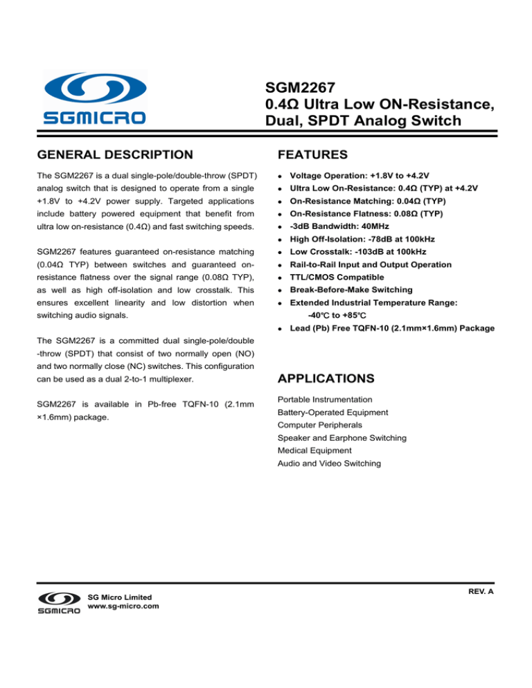
SGM2267 0.4Ω Ultra Low ON-Resistance, Dual, SPDT Analog Switch GENERAL DESCRIPTION FEATURES The SGM2267 is a dual single-pole/double-throw (SPDT) z Voltage Operation: +1.8V to +4.2V analog switch that is designed to operate from a single z Ultra Low On-Resistance: 0.4Ω (TYP) at +4.2V +1.8V to +4.2V power supply. Targeted applications z On-Resistance Matching: 0.04Ω (TYP) include battery powered equipment that benefit from z On-Resistance Flatness: 0.08Ω (TYP) ultra low on-resistance (0.4Ω) and fast switching speeds. z -3dB Bandwidth: 40MHz z High Off-Isolation: -78dB at 100kHz SGM2267 features guaranteed on-resistance matching z Low Crosstalk: -103dB at 100kHz (0.04Ω TYP) between switches and guaranteed on- z Rail-to-Rail Input and Output Operation resistance flatness over the signal range (0.08Ω TYP), z TTL/CMOS Compatible as well as high off-isolation and low crosstalk. This z Break-Before-Make Switching ensures excellent linearity and low distortion when z Extended Industrial Temperature Range: -40℃ to +85℃ switching audio signals. z Lead (Pb) Free TQFN-10 (2.1mm×1.6mm) Package The SGM2267 is a committed dual single-pole/double -throw (SPDT) that consist of two normally open (NO) and two normally close (NC) switches. This configuration can be used as a dual 2-to-1 multiplexer. SGM2267 is available in Pb-free TQFN-10 (2.1mm ×1.6mm) package. APPLICATIONS Portable Instrumentation Battery-Operated Equipment Computer Peripherals Speaker and Earphone Switching Medical Equipment Audio and Video Switching SG Micro Limited www.sg-micro.com REV. A 0.4Ω Ultra Low ON-Resistance, Dual, SPDT Analog Switch SGM2267 ORDERING INFORMATION MODEL PINPACKAGE SPECIFIED TEMPERATURE RANGE ORDERING NUMBER PACKAGE MARKING PACKAGE OPTION SGM2267 TQFN-10 (2.1mm×1.6mm) -40℃ to +85℃ SGM2267YTQD10/TR 2267 Tape and Reel, 3000 ABSOLUTE MAXIMUM RATINGS V+, IN to GND...............................................................0V to 4.6V (1) Analog, Digital voltage range .................... -0.3V to (V+) + 0.3V Continuous Current NO, NC, or COM.............................±250mA Peak Current NO, NC, or COM.......................................±350mA Operating Temperature Range.............................-40℃ to +85℃ Junction Temperature.........................................................150℃ Storage Temperature........................................-65℃ to +150℃ Lead Temperature (soldering, 10s)...................................260℃ ESD Susceptibility HBM..................................................................................4000V MM......................................................................................400V Stresses beyond those listed under “Absolute Maximum Ratings” may cause permanent damage to the device. These are stress ratings only, and functional operation of the device at these or any other conditions beyond those indicated in the operational sections of the specifications is not implied. Exposure to absolute maximum rating conditions for extended periods may affect device reliability. (1) Signals on NC, NO, or COM or IN exceeding V+ will be clamped by internal diodes. Limit forward diode current to maximum current ratings. CAUTION This integrated circuit can be damaged by ESD if you don’t pay attention to ESD protection. SGMICRO recommends that all integrated circuits be handled with appropriate precautions. Failure to observe proper handling and installation procedures can cause damage. ESD damage can range from subtle performance degradation to complete device failure. Precision integrated circuits may be more susceptible to damage because very small parametric changes could cause the device not to meet its published specifications. PIN CONFIGURATION (TOP VIEW) V+ COM1 IN1 IN2 COM2 9 8 7 6 5 10 1 NC1 2 3 4 NO1 NC2 NO2 GND PIN DESCRIPTION PIN 10 5 NAME V+ GND 8,7 IN1, IN2 9,6 2,4 1,3 COM1, COM2 NO1, NO2 NC1, NC2 FUNCTION Power supply Ground Digital control pin to connect the COM terminal to the NO or NC terminals Common terminal Normally-open terminal Normally-closed terminal TQFN-10 (2.1mm×1.6mm) Note: NO, NC and COM terminals may be an input or output. FUNCTION TABLE LOGIC 0 1 NO OFF ON NC ON OFF Switches Shown For Logic “0” Input SG Micro Limited www.sg-micro.com 2 0.4Ω Ultra Low ON-Resistance, Dual, SPDT Analog Switch SGM2267 ELECTRICAL CHARACTERISTICS (V+ = +4.2V, GND = 0V, VIH = +1.6V, VIL = +0.6V, TA = -40℃ to +85℃. Typical values are at V+ = +4.2V, TA = +25℃, unless otherwise noted.) PARAMETER SYMBOL CONDITIONS TEMP MIN -40°C to +85°C 0 TYP MAX UNITS ANALOG SWITCH Analog Signal Range VNO, VNC, VCOM 0.4 V 0.65 Ω 0.75 Ω RON V+ = 4.2V, 0V ≤ VNO or VNC ≤ V+, ICOM = -100mA, Test Circuit 1 -40°C to +85°C ∆RON V+ = 4.2V, 0V ≤ VNO or VNC ≤ V+, ICOM = -100mA, Test Circuit 1 -40°C to +85°C RFLAT(ON) V+ = 4.2V, 0V ≤ VNO or VNC ≤ V+, ICOM = -100mA, Test Circuit 1 0.12 Ω -40°C to +85°C 0.2 Ω On-Resistance On-Resistance Match Between Channels On-Resistance Flatness +25°C V+ +25°C 0.04 +25°C 0.08 0.15 Ω 0.2 Ω Source OFF Leakage Current INC(OFF), INO(OFF) V+ = 4.2V, VNO or VNC = 3.3 V/0.3V, VCOM = 0.3V/ 3.3V -40°C to +85°C 1 µA Channel ON Leakage Current INC(ON), INO(ON), ICOM(ON) V+ = 4.2 V, VCOM = 0.3V/ 3.3V, VNO or VNC = 0.3V/ 3.3V, or floating -40°C to +85°C 1 µA DIGITAL INPUTS Input High Voltage VINH -40°C to +85°C Input Low Voltage VINL -40°C to +85°C 0.5 V -40°C to +85°C 1 µA Input Leakage Current IIN V+ = 4.2V, VIN = 0V or 4.2V 1.6 V DYNAMIC CHARACTERISTICS VIN = 2.1V to 0V, RL = 50Ω, CL = 35pF, VNO1 or VNC1 = VNO2 or VNC2 = 2.1V, Test Circuit2 VIN = 2.1V to 0V, RL = 50Ω, CL = 35pF, VNO1 or VNC1 = VNO2 or VNC2 = 2.1V, Test Circuit2 VIN = 2.1V to 0V, RL = 50Ω, CL = 35pF, VNO1 or VNC1 = VNO2 or VNC2 = 2.1V, Test Circuit3 100kHz RL = 50Ω, Signal = 0dBm, Test Circuit4 1MHz +25°C -58 dB 100kHz +25°C -103 dB 1MHz +25°C -90 dB RL = 50Ω, Signal = 0dBm, Test Circuit6 +25°C 40.0 MHz Q VNO1 or VNC1 = VNO2 or VNC2 = 0V, CL = 1.0nF, Rs = 0Ω ,Test Circuit7 +25°C 4.0 pC Total Harmonic Distortion + Noise THD+N VCOM = 2VP-P, f = 20Hz to 20kHz, Test Circuit8 +25°C 0.011 % Channel ON Capacitance CON +25°C 106 pF Power Supply Range V+ -40°C to +85°C Power Supply Current I+ Turn-On Time tON Turn-Off Time tOFF Break-Before-Make Time Delay Off Isolation tD OISO Channel-to-Channel Crosstalk –3dB Bandwidth XTALK BW Charge Injection Select Input to Common I/O RL = 50Ω, Signal = 0dBm, Test Circuit5 +25°C 96 ns +25°C 16 ns +25°C 25 ns +25°C -78 dB POWER REQUIREMENTS V+ = 4.2V, VIN = 0V or V+ -40°C to +85°C 1.8 4.2 V 1 µA Specifications subject to changes without notice. SG Micro Limited www.sg-micro.com 3 0.4Ω Ultra Low ON-Resistance, Dual, SPDT Analog Switch SGM2267 ELECTRICAL CHARACTERISTICS (V+ = +2.7V to +3.6V, GND = 0V, VIH = +1.6V, VIL = +0.4V, TA = -40℃ to +85℃. Typical values are at V+ = +3.0V, TA = +25℃, unless otherwise noted.) PARAMETER SYMBOL CONDITIONS TEMP MIN -40°C to +85°C 0 TYP MAX UNITS V+ V 0.5 0.7 Ω 0.8 Ω 0.03 0.15 Ω 0.2 Ω 0.1 0.18 Ω -40°C to +85°C 0.2 Ω ANALOG SWITCH Analog Signal Range On-Resistance On-Resistance Match Between Channels VNO, VNC, VCOM RON ∆RON V+ = 2.7V, 0V ≤ VNO or VNC ≤ V+, ICOM = -100mA, Test Circuit 1 V+ = 2.7V, 0V ≤ VNO or VNC ≤ V+, ICOM = -100mA, Test Circuit 1 +25°C -40°C to +85°C +25°C -40°C to +85°C +25°C On-Resistance Flatness RFLAT(ON) V+ = 2.7V, 0V ≤ VNO or VNC ≤ V+, ICOM = -100mA, Test Circuit 1 Source OFF Leakage Current INC(OFF), INO(OFF) V+ = 3.6V, VNO or VNC = 3.3V/ 0.3V, VCOM = 0.3V/ 3.3V -40°C to +85°C 1 µA INC(ON), INO(ON), V+ = 3.6V, VCOM = 0.3V/ 3.3V, ICOM(ON) VNO or VNC = 0.3V/ 3.3V, or floating -40°C to +85°C 1 µA Channel ON Leakage Current DIGITAL INPUTS Input High Voltage VINH Input Low Voltage VINL Input Leakage Current IIN -40°C to +85°C V+ = 2.7V, VIN = 0V or 2.7V 1.5 V -40°C to +85°C 0.4 V -40°C to +85°C 1 µA DYNAMIC CHARACTERISTICS Turn-On Time tON VIN =1.5V to 0V, RL = 50Ω, CL = 35pF, VNO1 or VNC1 = VNO2 or VNC2 = 1.5V, Test Circuit2 +25°C 100 ns Turn-Off Time tOFF VIN = 1.5V to 0V, RL = 50Ω, CL = 35pF, VNO1 or VNC1 = VNO2 or VNC2 = 1.5V, Test Circuit2 +25°C 25 ns tD VIN = 1.5V to 0V, RL = 50Ω, CL = 35pF, VNO1 or VNC1 = VNO2 or VNC2 =1.5V, Test Circuit3 +25°C 28 ns Break-Before-Make Time Delay Off Isolation OISO RL = 50Ω, Signal = 0dBm, Test Circuit4 100kHz +25°C -78 dB 1MHz +25°C -58 dB Channel-to-Channel Crosstalk XTALK RL = 50Ω, Signal = 0dBm, Test Circuit5 100kHz +25°C -103 dB 1MHz +25°C -90 dB BW RL = 50Ω, Signal = 0dBm, Test Circuit6 +25°C 40 MHz Q VNO1 or VNC1 = VNO2 or VNC2 = 0V, CL=1.0nF, RS = 0Ω, Test Circuit7 +25°C 4.0 pC THD+N VCOM =1.5VP-P, f = 20Hz to 20kHz, Test Circuit8 +25°C 0.015 % +25°C 106 pF –3dB Bandwidth Charge Injection Select Input to Common I/O Total Harmonic Distortion + Noise Channel ON Capacitance CON Specifications subject to changes without notice. SG Micro Limited www.sg-micro.com 4 0.4Ω Ultra Low ON-Resistance, Dual, SPDT Analog Switch SGM2267 TYPICAL PERFORMANCE CHARACTERISTICS On Response vs. Frequency On Response vs. Frequency 3 3 V+ = +3V TA = +25℃ 0 On Response (dB) On Response (dB) V+ = +4.2V TA = +25℃ -3 -6 0 -3 -6 -9 -9 0.1 1 10 100 Frequency (MHz) 0.1 1000 1 Response vs. Frequency 20 0 0 -20 -20 OFF-ISOLATION -60 CROSSTALK -80 -100 V+ = +4.2V TA = +25℃ -120 -140 0.01 0.1 1 10 Frequency (MHz) SG Micro Limited www.sg-micro.com 100 1000 On Response (dB) On Response (dB) 1000 Response vs. Frequency 20 -40 10 100 Frequency (MHz) -40 OFF-ISOLATION -60 CROSSTALK -80 -100 V+ = +3V TA = +25℃ -120 -140 0.01 0.1 1 10 Frequency (MHz) 100 1000 5 0.4Ω Ultra Low ON-Resistance, Dual, SPDT Analog Switch SGM2267 TEST CIRCUITS 100mA V1 NO or NC COM VNO or VNC RON = V1/100mA Test Circuit 1. On Resistance V+ V+ NC 0.1μF 50% COM NO VOUT CL 35pF RL 50Ω IN VOH 50% 90% 90% VOL GND tOFF tON Test Circuit 2. Switching Times (tON, tOFF) V+ 0.1μF V+ NC VIN COM NO VOUT RL 50Ω IN GND CL 35pF 50% 0 90% of VOH VOUT 0 tD Test Circuit 3. Break-Before-Make Time (tD) SG Micro Limited www.sg-micro.com 6 0.4Ω Ultra Low ON-Resistance, Dual, SPDT Analog Switch SGM2267 TEST CIRCUITS (Cont.) V+ 0.1µF V+ NC NO VOUT COM RL 50Ω Source Signal RL 50Ω CL 5pF IN GND Test Circuit 4. Off Isolation V+ 0.1μF V+ NO or NC Source Signal COM RL 50Ω IN1 CL 5pF IN2 NO or NC N.C. COM VOUT RL 50Ω GND Channel To Channel Crosstalk= -20 × log CL 5pF VNO or VNC VOUT Test Circuit 5. Channel-to-Channel Crosstalk SG Micro Limited www.sg-micro.com 7 0.4Ω Ultra Low ON-Resistance, Dual, SPDT Analog Switch SGM2267 TEST CIRCUITS (Cont.) V+ 0.1μF V+ NO or NC Source Signal COM VOUT CL 5pF IN GND Test Circuit 6. -3dB Bandwidth V+ NC RS VS 0 COM NO VOUT CL 1nF IN ΔOUT VOUT GND Q = ΔVOUT × CL Test Circuit 7. Charge Injection (Q) V+ RL 600Ω 0.1μF Audio Analyzer Source Signal V+ /2 600Ω COM NC 600Ω 10μF NO 10μF CL 50pF IN VIN GND 100kΩ 600Ω Test Circuit 8. Total Harmonic Distortion SG Micro Limited www.sg-micro.com 8 0.4Ω Ultra Low ON-Resistance, Dual, SPDT Analog Switch SGM2267 PACKAGE OUTLINE DIMENSIONS TQFN-10 (2.1mm×1.6mm) 2.100±0.050 0.400±0.050 (×9) 0.500 Bsc 1.600±0.050 0.800 Ref. 0.15 0.200±0.050 PIN #1 DOT BY MARKING 2 1 1.500 Ref. TOP VIEW 0.08 PIN #1 IDENTIFICATION BOTTOM VIEW 0.750±0.050 0.000-0.050 0.203 Ref. SIDE VIEW Note: All linear dimensions are in millimeters. 12/2008 REV. A SGMICRO is dedicated to provide high quality and high performance analog IC products to customers. All SGMICRO products meet the highest industry standards with strict and comprehensive test and quality control systems to achieve world-class consistency and reliability. For information regarding SGMICRO Corporation and its products, see www.sg-micro.com SG Micro Limited www.sg-micro.com 9
