HCPL-9000/-0900, -9030/-0930,
HCPL-9031/-0931, -900J/-090J,
HCPL-901J/-091J, -902J/-092J
High Speed Digital Isolators
Data Sheet
Lead (Pb) Free
RoHS 6 fully
compliant
RoHS 6 fully compliant options available;
-xxxE denotes a lead-free product
Description
Features
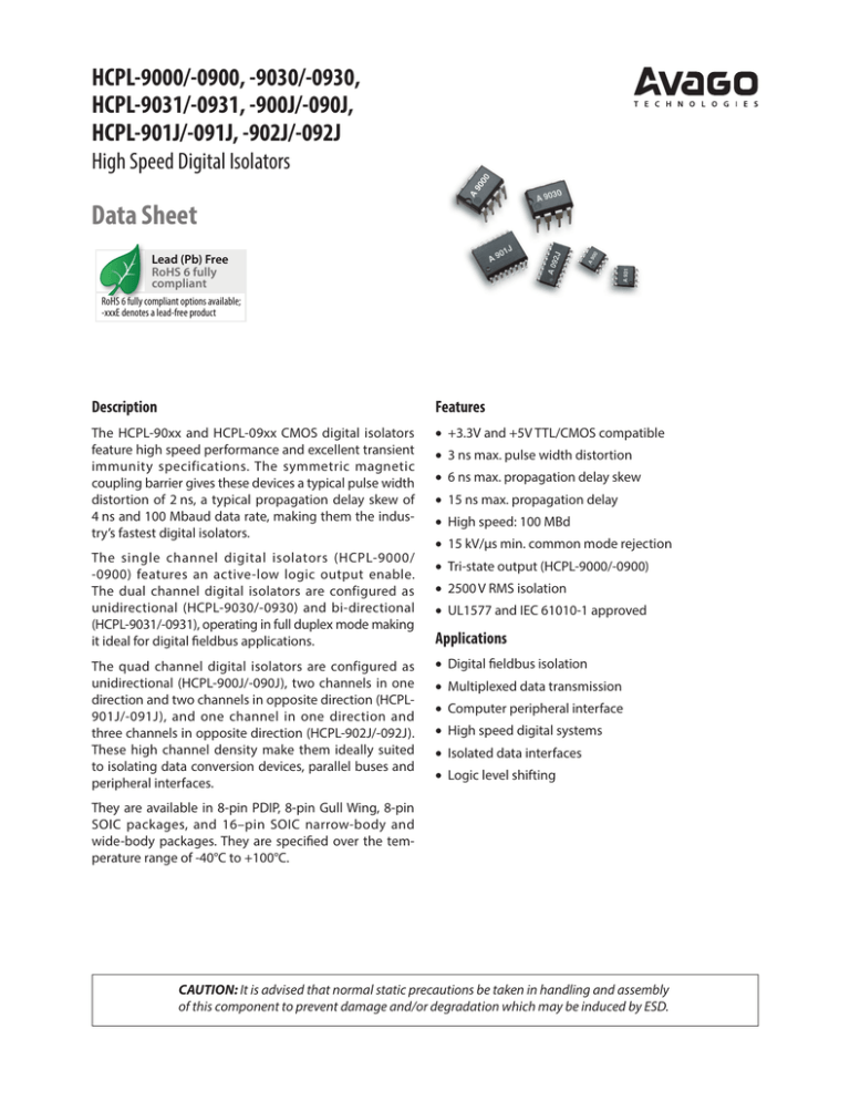
The HCPL-90xx and HCPL-09xx CMOS digital isolators
feature high speed performance and excellent transient
immunity specifications. The symmetric magnetic
coupling barrier gives these devices a t­ ypical pulse width
distortion of 2 ns, a typical propagation delay skew of
4 ns and 100 Mbaud data rate, making them the industry’s fastest digital isolators.
• +3.3V and +5V TTL/CMOS compatible
The single channel digital isolators (HCPL-9000/
-0900) features an active-low logic output enable.
The dual channel digital isolators are configured as
­unidirectional (HCPL-9030/-0930) and bi-directional
(HCPL-9031/-0931), operating in full duplex mode making
it ideal for digital fieldbus applications.
The quad channel digital isolators are configured as
unidirectional (HCPL-900J/-090J), two channels in one
direction and two channels in opposite direction (HCPL901J/-091J), and one channel in one direction and
three channels in opposite direction (HCPL-902J/-092J).
These high channel density make them i­deally suited
to isolating data conversion devices, parallel buses and
peripheral interfaces.
• 3 ns max. pulse width distortion
• 6 ns max. propagation delay skew
• 15 ns max. propagation delay
• High speed: 100 MBd
• 15 kV/µs min. common mode rejection
• Tri-state output (HCPL-9000/-0900)
• 2500 V RMS isolation
• UL1577 and IEC 61010-1 approved
Applications
• Digital fieldbus isolation
• Multiplexed data transmission
• Computer peripheral interface
• High speed digital systems
• Isolated data interfaces
• Logic level shifting
They are available in 8-pin PDIP, 8-pin Gull Wing, 8‑pin
SOIC packages, and 16–pin SOIC narrow-body and
wide-body packages. They are specified over the temperature range of -40°C to +100°C.
CAUTION: It is advised that normal static precautions be taken in handling and assembly
of this component to prevent damage and/or degradation which may be induced by ESD.
Selection Guide
Device Number
Channel Configuration
Package
HCPL-9000
Single
8-pin DIP (300 Mil)
HCPL-0900
Single
8-pin Small Outline
HCPL-9030
Dual
8-pin DIP (300 Mil)
HCPL-0930
Dual
8-pin Small Outline
HCPL-9031
Dual, Bi-Directional
8-pin DIP (300 Mil)
HCPL-0931
Dual, Bi-Directional
8-pin Small Outline
HCPL-900J
Quad
16-pin Small Outline, Wide Body
HCPL-090J
Quad
16-pin Small Outline, Narrow Body
HCPL-901J
Quad, 2/2, Bi-Directional
16-pin Small Outline, Wide Body
HCPL-091J
Quad, 2/2, Bi-Directional
16-pin Small Outline, Narrow Body
HCPL-902J
Quad, 1/3, Bi-Directional
16-pin Small Outline, Wide Body
HCPL-092J
Quad, 1/3, Bi-Directional
16-pin Small Outline, Narrow Body
Ordering Information
HCPL-09xx and HCPL-90xx are UL Recognized with 2500 Vrms for 1 minute per UL1577.
Part number
Option
RoHS
Compliant
HCPL-9000
HCPL-9030
HCPL-9031
-000E
HCPL-0900
HCPL-0930
HCPL-0931
HCPL-900J
HCPL-901J
HCPL-902J
HCPL-090J
HCPL-091J
HCPL-092J
Non RoHS
Compliant
Package
Surface Mount
Gull
Wing
Tape &
Reel
No option
300mil
Quantity
50 per tube
DIP-8
-300
X
X
50 per tube
-500E
-500
X
X
X
1000 per reel
-000E
X
100 per tube
-500E
No option
SO-8
-500
X
1500 per reel
-000E
No option
Wide Body
X
50 per tube
X
1000 per reel
No option
Narrow Body
X
50 per tube
X
1000 per reel
-300E
-500E
-000E
-500E
-500
SO-16
SO-16
-500
X
X
X
To order, choose a part number from the part number column and combine with the desired option from the option
column to form an order entry.
Example 1:
HCPL-9031-500E to order product of 300mil DIP Gull Wing Surface Mount package in Tape and Reel in RoHS
compliant.
Example 2:
HCPL-0900 to order product of SO-8 package in tube packaging and non RoHS compliant.
Option datasheets are available. Contact your Avago sales representative or authorized distributor for information.
2
Functional Diagrams
SymbolDescription
Single Channel
VDD1
Power Supply 1
VDD2
Power Supply 2
INX
Logic Input Signal
OUTX
Logic Output Signal
GND1
Power Supply Ground 1
GND2
Power Supply Ground 2
VOE
Logic Output Enable (Single Channel), Active Low
NC
Not Connected
VDD1
1
IN1
2
NC
3
GND1
4
Galvanic Isolation
Pin Description
8
VDD2
7
VOE
6
OUT1
5
GND2
Truth Table
IN1
VOE
OUT1
L
L
L
H
L
H
L
H
Z
H
H
Z
HCPL-9000/0900
1
IN1
2
IN2
3
GND1
4
8
VDD2
VDD1
1
7
OUT1
IN1
2
6
OUT2
OUT2
3
5
GND2
GND1
4
HCPL-9030/0930
Galvanic Isolation
VDD1
Galvanic Isolation
Dual Channel
8
VDD2
7
OUT1
6
IN2
5
GND2
HCPL-9031/0931
Quad Channel
VDD2
VDD1
1
16
VDD2
VDD1
1
16
VDD2
GND1
2
15
GND2
GND1
2
15
GND2
GND1
2
15
GND2
IN1
3
14
OUT1
IN1
3
14
OUT1
IN1
3
14
OUT1
IN2
4
13
OUT2
IN2
4
13
OUT2
IN2
4
13
OUT2
IN3
5
12
OUT3
OUT3
5
12
IN3
IN3
5
12
OUT3
IN4
6
11
OUT4
OUT4
6
11
IN4
OUT4
6
11
IN4
NC
7
10
NC
NC
7
10
NC
NC
7
10
NC
GND1
9
GND1
9
GND2
GND2
8
9
GND1
8
8
GND2
HCPL-900J/-090J
3
HCPL-901J/-091J
Galvanic Isolation
16
Galvanic Isolation
1
Galvanic Isolation
VDD1
HCPL-902J/-092J
Package Outline Drawings
HCPL-9000, HCPL-9030 and HCPL-9031 Standard DIP Packages
8
7
6
5
0.240 (6.096)
0.260 (6.604)
1
2
3
4
0.360 (9.000)
0.400 (10.160)
0.55 (1.397)
0.65 (1.651)
0.290 (7.366)
0.310 (7.874)
0.120 (3.048)
0.150 (3.810)
0.008 (0.203)
0.015 (0.381)
0.015 (0.381)
0.035 (0.889)
°
0.030 (0.762)
0.045 (1.143)
0.015 (0.380)
0.023 (0.584)
0.300 (7.620)
0.370 (9.398)
0.090 (2.286)
0.110 (2.794)
0.045 (1.143)
0.065 (1.651)
3°
8°
DIMENSIONS: INCHES (MILLIMETERS) MIN
MAX
HCPL-9000, HCPL-9030 and HCPL-9031 Gull Wing Surface Mount Option 300
PAD LOCATION (for reference only)
0.040 (1.016)
0.047 (1.194)
0.360 (9.000)
0.400 (10.160)
8
7
6
5
0.190 TYP.
(4.826)
0.240 (6.096)
0.260 (6.604)
1
2
3
0.370 (9.398)
0.390 (9.906)
4
0.047 (1.194)
0.070 (1.778)
0.045 (1.143)
0.065 (1.651)
0.030 (0.762)
0.045 (1.143)
0.370 (9.400)
0.390 (9.900)
0.290 (7.370)
0.310 (7.870)
0.120 (3.048)
0.150 (3.810)
0.030 (0.760)
0.056 (1.400)
0.100
(2.540)
BSC
MIN
MAX
LEAD COPLANARITY = 0.004 INCHES (0.10 mm)
DIMENSIONS INCHES (MILLIMETERS)
4
0.025 (0.632)
0.035 (0.892)
0.015 (0.385)
0.035 (0.885)
0.015 (0.381)
0.025 (0.635)
0.008 (0.203)
0.013 (0.330)
12° NOM.
HCPL-0900, HCPL-0930 and HCPL-0931 Small Outline SO-8 Package
0.189 (4.80)
0.197 (5.00)
8
7
6
5
0.228 (5.80)
0.244 (6.20)
0.150 (3.80)
0.157 (4.00)
1
2
3
4
0.013 (0.33)
0.020 (0.51)
0.010 (0.25)
0.020 (0.50)
x 45°
0.008 (0.19)
0.010 (0.25)
0.004 (0.10)
0.010 (0.25)
0.054 (1.37)
0.069 (1.75)
0.040 (1.016)
0.060 (1.524)
0.016 (0.40)
0.050 (1.27)
DIMENSIONS: INCHES (MILLIMETERS) MIN
MAX
HCPL-900J, HCPL-901J and HCPL-902J Wide Body SOIC-16 Package
0.397 (10.084)
0.413 (10.490)
8
Pin 1 indent
1
0.394 (10.007)
0.419 (10.643)
0.013 (0.330)
0.020 (0.508)
0.092 (2.337)
0.105 (2.670)
7° TYP
7° TYP
0.287 (7.290)
0.300 (7.620)
0.080 (2.032)
0.100 (2.54)
0.040 (1.016)
0.060 (1.524)
DIMENSIONS: INCHES (MILLIMETERS)
5
0.004 (0.1016)
0.012 (0.300)
MIN
MAX
0.007 (0.200)
0.013 (0.330)
0.016 (0.40)
0.050 (1.27)
HCPL-090J, HCPL-091J and HCPL-092J Narrow Body SOIC-16 Package
0.386 (9.802)
0.394 (9.999)
Pin 1 indent
1
8
0.228 (5.791)
0.244 (6.197)
0.152 (3.861)
0.157 (3.988)
0.013 (0.330)
0.020 (0.508)
0.054 (1.372)
0.072 (1.800)
0.007 (0.200)
0.013 (0.330)
0.040 (1.020)
0.050 (1.270)
0.040 (1.016)
0.060 (1.524)
DIMENSIONS: INCHES (MILLIMETERS)
0.016 (0.406)
0.050 (1.270)
0.004 (0.102)
0.012 (0.300)
MIN
MAX
Package Characteristics
Parameter
Symbol
Min.
Typ.
Max.
Capacitance (Input-Output) [1]CI-O
Single Channel
1.1
Dual Channel
2.0
Quad Channel
4.0
Units
Test Conditions
pF
f = 1 MHz
Thermal Resistance
θJCT
°C/W
8-Pin PDIP
54
8-Pin SOIC
144
16-Pin SOIC Narrow Body 41
16-Pin SOIC Wide Body
28
Thermocouple located at center underside of package
Package Power Dissipation
PPD
mW
8-Pin PDIP
150
8-Pin SOIC
150
16-Pin SOIC Narrow Body
150
16-Pin SOIC Wide Body
150
Notes:
1. Single and dual channels device are considered two-terminal devices: pins 1-4 shorted and pins 5-8 shorted. Quad channel devices are considered two‑terminal devices: pins 1-8 shorted and pins 9-16 shorted.
This product has been tested for electrostatic sensitivity to the limits stated in the specifications. However, Avago recommends that all integrated circuits be handled with appropriate care to avoid damage. Damage caused by inappropriate handling or storage could range from
performance degradation to complete failure.
6
Insulation and Safety Related Specifications
Parameters
ConditionMin.
Typ.
Max.
Units
Barrier ImpedanceΩ||pF
Single Channel
>1014||3
Dual Channel
>1014||3
Quad Channel
>1014||7
Creepage Distance (External)mm
8-Pin PDIP
8-Pin SOIC
16-Pin SOIC Narrow Body
16-Pin SOIC Wide Body
Leakage Current
7.04 4.04
4.03 8.08
240 VRMS
60 Hz
0.2
µA
IEC61010-1 Insulation Characteristics*
Description
Symbol
HCPL-0900
HCPL-0930
HCPL-090J
HCPL-091J
HCPL-092J
HCPL-9000
HCPL-9030
HCPL-900J
HCPL-901J
HCPL-902J
I – III
I – IV
Units
Installation classification per DIN VDE 0110/1.89, Table 1
for rated mains voltage ≤ 150 Vrms
for rated mains voltage ≤ 300 Vrms
I – III
Pollution Degree (DIN VDE 0110/1.89)
Maximum Working Insulation Voltage
VIORM
2
2
150
300
Soldering Profile
The recommended reflow soldering conditions are per JEDEC Standard J-STD-020 (latest revision).
7
Vrms
Absolute Maximum Ratings
ParametersSymbol
Storage Temperature
Min.
Max.
Units
TS –55150°C
Ambient Operating Temperature TA –55125°C
[1]
Supply Voltage
VDD1, VDD2–0.5
Input Voltage
VIN –0.5VDD1 +0.5
V
Voltage Output Enable (HCPL-9000/-0900)
VOE–0.5VDD2 +0.5
V
Output Voltage
VOUT–0.5 VDD2 +0.5
V
Output Current Drive
IOUT
Lead Solder Temperature (10s)
ESD
7
V
10 mA
260
°C
2 kV Human Body Model
Notes:
1. Absolute Maximum ambient operating temperature means the device will not be damaged if operated under these conditions. It does not
guarantee performance.
Recommended Operating Conditions
Parameters
SymbolMin.
Max. Units
Ambient Operating Temperature
TA –40100°C
Supply Voltage
VDD1, VDD2
3.05.5V
Logic High Input Voltage
VIH 2.4VDD1V
Logic Low Input Voltage
VIL 0 0.8V
Input Signal Rise and Fall Times
tIR, tIF
1
µs
This product has been tested for electrostatic sensitivity to the limits stated in the specifications. However, Avago recommends
that all integrated circuits be handled with appropriate care to avoid damage. Damage caused by inappropriate handling or storage could range from performance degradation to complete failure.
8
3.3V operation: Electrical Specifications
Test conditions that are not specified can be anywhere within the recommended operating range.
All typical specifications are at TA=+25°C, VDD1 = VDD2 = +3.3 V.
Parameter
Symbol
Min.
Typ.
Max.
Units Test Conditions
Quiescent Supply Current 1
IDD1
mAVIN = 0V
HCPL-9000/-0900
0.008
0.01
HCPL-9030/-0930
0.008
0.01
HCPL-9031/-0931 1.52.0
HCPL-900J/-090J 0.0180.02
HCPL-901J/-091J 3.34.0
HCPL-902J/-092J
1.5
2.0
Quiescent Supply Current 2
IDD2
mA
VIN = 0V
HCPL-9000/-0900
HCPL-9030/-0930
HCPL-9031/-0931
HCPL-900J/-090J
HCPL-901J/-091J
HCPL-902J/-092J
Logic Input Current
IIN
Logic High Output Voltage
VOH
Logic Low Output Voltage
3.3
4.0
3.3
4.0
1.52.0
5.58.0
3.34.0
3.0
6.0
-10
VDD2 ­– 0.1
0.8*VDD2
10
VDD2
VDD2 – 0.5
µA
VIOUT = -20 µA, VIN = VIH
V
IOUT = -4 mA, VIN = VIH
VOL
0
0.1
V
IOUT = 20 µA, VIN = VIL
0.5
0.8
V
IOUT = 4 mA, VIN= VIL
MBd
CL = 15 pF
Switching Specifications
Maximum Data Rate
100
110
Clock Frequency
fmax
50
Propagation Delay Time to Logic
Low Output
tPHL
12
18ns
Propagation Delay Time toLogic
High Output
tPLH
12
18
Pulse Width
tPW
10
MHz
ns
ns
Pulse Width Distortion [1]
|PWD|
|tPHL – tPLH|
2
3ns
Propagation Delay Skew [2]tPSK
4
6ns
Output Rise Time (10 – 90%)
tR
2
4ns
Output Fall Time (10 – 90%)
tF
2
4ns
Propagation Delay Enable to Output (Single Channel)
High to High Impedance
tPHZ
3
5ns
Low to High Impedance
tPLZ
3
5
High Impedance to High
tPZH
3
5ns
High Impedance to Low
tPZL
3
5
2
3ns
Channel-to-Channel Skew tCSK
(Dual and Quad Channels)
Common Mode Transient Immunity |CMH|
15
18
(Output Logic High or Logic Low)[3]|CML|
Notes:
ns
ns
kV/µsVcm = 1000V
1. PWD is defined as |tPHL -tPLH|. %PWD is equal to the PWD divided by the pulse width.
2.tPSK is equal to the magnitude of the worst case difference in tPHL and/or tPLH that will be seen between units at 25°C.
3.CMH is the maximum common mode voltage slew rate that can be sustained while maintaining VOUT > 0.8VDD2. CML is the maximum common mode
input voltage that can be sustained while maintaining VOUT < 0.8V. The common mode voltage slew rates apply to both rising and falling common mode
voltage edges.
This product has been tested for electrostatic sensitivity to the limits stated in the specifications. However, Avago recommends that all integrated circuits
be handled with appropriate care to avoid damage. Damage caused by inappropriate handling or storage could range from performance degradation to
complete failure.
9
5V operation: Electrical Specifications
Test conditions that are not specified can be anywhere within the recommended operating range.
All typical specifications are at TA=+25°C, VDD1 = VDD2 = +5.0 V.
Parameter
Symbol
Min.
Typ.
Max.
Units Test Conditions
Quiescent Supply Current 1
IDD1
mAVIN = 0V
HCPL-9000/-0900
0.012
0.018
HCPL-9030/-0930
0.012
0.018
HCPL-9031/-0931 2.53.0
HCPL-900J/-090J 0.0240.036
HCPL-901J/-091J 5.06.0
HCPL-902J/-092J
2.5
3.0
Quiescent Supply Current 2
IDD2
mA
VIN = 0V
HCPL-9000/-0900
HCPL-9030/-0930
HCPL-9031/-0931
HCPL-900J/-090J
HCPL-901J/-091J
HCPL-902J/-092J
Logic Input Current
IIN
Logic High Output Voltage
VOH
Logic Low Output Voltage
5.0
6.0
5.0
6.0
2.53.0
8.012.0
5.06.0
6.0
9.0
-10
10
µA
VDD2 – 0.1
VDD2
VIOUT = -20 µA, VIN = VIH
0.8*VDD2
VDD2 – 0.5
VIOUT = -4 mA, VIN = VIH
VOL
0
0.1
V
IOUT = 20 µA, VIN = VIL
0.5
0.8
V
IOUT = 4 mA, VIN= VIL
MBd
CL = 15 pF
Switching Specifications
Maximum Data Rate
100
110
Clock Frequency
fmax
50
Propagation Delay Time to Logic
Low Output
tPHL
10
15ns
Propagation Delay Time to Logic
High Output
tPLH
10
15
Pulse Width
tPW
10
MHz
ns
ns
Pulse Width Distortion [1]
|PWD|
|tPHL – tPLH|
2
3ns
Propagation Delay Skew[2]tPSK
4
6ns
Output Rise Time (10 – 90%)
tR
1
3ns
Output Fall Time (10 – 90%)
tF
1
3ns
Propagation Delay Enable to Output (Single Channel)
High to High Impedance
tPHZ
3
5ns
Low to High Impedance
tPLZ
3
5
High Impedance to High
tPZH
3
5ns
High Impedance to Low
tPZL
3
5
2
3ns
Channel-to-Channel Skew tCSK
(Dual and Quad Channels)
Common Mode Transient Immunity |CMH|
15
18
(Output Logic High or Logic Low)[3]|CML|
Notes:
ns
ns
kV/µsVcm = 1000V
1. PWD is defined as |tPHL -tPLH|. %PWD is equal to the PWD divided by the pulse width.
2.tPSK is equal to the magnitude of the worst case difference in tPHL and/or tPLH that will be seen between units at 25°C.
3.CMH is the maximum common mode voltage slew rate that can be sustained while maintaining VOUT > 0.8VDD2. CML is the maximum common mode
input voltage that can be sustained while maintaining VOUT < 0.8V. The common mode voltage slew rates apply to both rising and falling common mode
voltage edges.
This product has been tested for electrostatic sensitivity to the limits stated in the specifications. However, Avago recommends that all integrated circuits
be handled with appropriate care to avoid damage. Damage caused by inappropriate handling or storage could range from performance degradation to
complete failure.
10
Mixed 5V/3.3V or 3.3V/5V operation: Electrical Specifications
Test conditions that are not specified can be anywhere within the recommended operating range.
All typical specifications are at TA=+25°C, VDD1 = +5.0 V, VDD2 = +3.3V.
Parameter
Symbol
Min.
Typ.
Max.
Units Test Conditions
HCPL-9000/-0900
IDD1
0.012
0.018
HCPL-9030/-0930
0.012
0.018
HCPL-9031/-0931 2.53.0
HCPL-900J/-090J 0.0240.036
HCPL-901J/-091J 5.06.0
HCPL-902J/-092J 2.53.0
Quiescent Supply Current 2
IDD2
mA
VIN = 0V
HCPL-9000/-0900
HCPL-9030/-0930
HCPL-9031/-0931
HCPL-900J/-090J
HCPL-901J/-091J
HCPL-902J/-092J
Logic Input Current
IIN
Logic High Output Voltage
VOH
Logic Low Output Voltage
5.0
6.0
5.0
6.0
2.53.0
8.012.0
5.06.0
6.0
9.0
-10
10
µA
VDD2 – 0.1
VDD2
VIOUT = -20 µA, VIN = VIH
0.8*VDD2
VDD2 – 0.5
VIOUT = -4 mA, VIN = VIH
VOL
0
0.1
V
IOUT = 20 µA, VIN = VIL
0.5
0.8
V
IOUT = 4 mA, VIN= VIL
MBd
CL = 15 pF
Switching Specifications
Maximum Data Rate
100
110
Clock Frequency
fmax
50
Propagation Delay Time to Logic
Low Output
tPHL
12
18ns
Propagation Delay Time to Logic
High Output
tPLH
12
18
Pulse Width
tPW
10
MHz
ns
ns
Pulse Width Distortion [1]
|PWD|
|tPHL – tPLH|
2
3ns
Propagation Delay Skew[2]tPSK
4
6ns
Output Rise Time (10 – 90%)
tR
2
4ns
Output Fall Time (10 – 90%)
tF
2
4ns
Propagation Delay Enable to Output (Single Channel)
High to High Impedance
tPHZ
3
5ns
Low to High Impedance
tPLZ
3
5
High Impedance to High
tPZH
3
5ns
High Impedance to Low
tPZL
3
5
2
3ns
Channel-to-Channel Skew tCSK
(Dual and Quad Channels)
Common Mode Transient Immunity |CMH|
15
18
(Output Logic High or Logic Low)[3]|CML|
Notes:
ns
ns
kV/µsVcm = 1000V
1. PWD is defined as |tPHL -tPLH|. %PWD is equal to the PWD divided by the pulse width.
2.tPSK is equal to the magnitude of the worst case difference in tPHL and/or tPLH that will be seen between units at 25°C.
3.CMH is the maximum common mode voltage slew rate that can be sustained while maintaining VOUT > 0.8VDD2. CML is the maximum common mode
input voltage that can be sustained while maintaining VOUT < 0.8V. The common mode voltage slew rates apply to both rising and falling common mode
voltage edges.
This product has been tested for electrostatic sensitivity to the limits stated in the specifications. However, Avago recommends that all integrated circuits
be handled with appropriate care to avoid damage. Damage caused by inappropriate handling or storage could range from performance degradation to
complete failure.
11
Applications Information
Bypassing and PC Board Layout
Power Consumption
The HCPL-90xx and HCPL-09xx digital isolators are
extremely easy to use. No external interface circuitry is
required because the isolators use high-speed CMOS IC
technology allowing CMOS logic to be connected directly
to the inputs and outputs. As shown in Figure 1, the only
external components required for proper operation are
two 47 nF ceramic capacitors for decoupling the power
supplies. For each capacitor, the total lead length between
both ends of the capacitor and the power-supply pins
should not exceed 20 mm. Figure 2 illustrates the recommended printed circuit board layout for the HCPL-9000
or HCPL-0900. For data rates in excess of 10MBd, use of
ground planes for both GND1 and GND2 is highly recommended.
The HCPL-90xx and HCPL-09xx CMOS digital isolators
achieves low power consumption from the ­manner by
which they transmit data across isolation barrier. By
detecting the edge transitions of the input logic signal
and converting this to a narrow current pulse, which
drives the isolation barrier, the isolator then latches the
input logic state in the output latch. Since the current
pulses are narrow, about 2.5 ns wide, the power consumption is independent of mark-to-space ratio and solely
dependent on frequency.
The approximate power supply current per channel is:
I(Input) = 40(f/fmax)(1/4) mA
where f = operating frequency, fmax = 50 MHz.
Signal Status on Start-up and Shut Down
To minimize power dissipation, the input signals to the
channels of HCPL-90xx and HCPL-09xx digital isolators
are differentiated and then latched on the output side of
the isolation barrier to reconstruct the signal. This could
result in an ambiguous output state depending on power
up, shutdown and power loss sequencing. Therefore, the
designer should consider the inclusion of an initialization signal in this start-up circuit. Initialization consists of
toggling the input either high then low or low then high.
VDD1
C2
2
NC 3
GND1
HCPL-9000
or
HCPL-0900
IN1
VDD2
8
1
C1
4
7
VOE
OUT1
6
5
GND2
Note: C1, C2 = 47 nF ceramic capacitors
Figure 1. Functional Diagram of Single Channel HCPL-0900 or HCPL-0900.
VDD1
VDD2
C1
HCPL-9000
or
HCPL-0900
IN1
GND1
Figure 2. Recommended Printed Circuit Board Layout.
12
VOE
C2
OUT1
GND2
Propagation Delay, Pulse Width Distortion and Propagation Delay Skew
Propagation Delay is a figure of merit, which describes
how quickly a logic signal propagates through a system
as illustrated in Figure 3.
5 V CMOS
INPUT
VIN
50%
0V
tPLH
OUTPUT
VOUT
90%
10%
tPHL
90%
10%
VOH
2.5 V CMOS
VOL
As illustrated in Figure 4, if the inputs of two or more
devices are switched either ON or OFF at the same time,
tPSK is the difference between the minimum propagation
delay, either tPLH or tPHL, and the maximum propagation
delay, either tPLH or tPHL.
VIN
50%
2.5 V
CMOS
VOUT
tPSK
Figure 3. Timing Diagrams to Illustrate Propagation Delay, tPLH and tPHL.
The propagation delay from low to high, t PLH , is the
amount of time required for an input signal to propagate
to the output, causing the output to change from low to
high. Similarly, the propagation delay from high to low,
tPHL, is the amount of time required for the ­input signal to
propagate to the output, causing the output to change
from high to low.
Pulse Width Distortion, PWD, is the difference between tPHL
and tPLH and often determines the maximum data rate capability of a transmission system. PWD can be expressed in
percent by dividing the PWD (in ns) by the minimum pulse
width (in ns) being transmitted. Typically, PWD on the order
of 20 – 30% of the minimum pulse width is tolerable.
Propagation Delay Skew, tPSK, and Channel-to-Channel
Skew, tCSK, are critical parameters to consider in parallel
data transmission applications where s­ ynchronization of
signals on parallel data lines is a concern. If the parallel
data is being sent through channels of the digital
isolators, differences in propagation delays will cause
the data to arrive at the o
­ utputs of the digital isolators
at different times. If this difference in propagation delay
is large enough, it will limit the maximum transmission
rate at which parallel data can be sent through the digital
isolators.
tPSK is defined as the difference between the minimum and
maximum propagation delays, either tPLH or tPHL, among two
or more devices which are operating u
­ nder the same conditions (i.e., the same drive current, ­supply voltage, output
load, and operating temperature). tCSK is defined as the
difference between the minimum and maximum propagation delays, either tPLH or tPHL, among two or more channels
within a single device (applicable to dual and quad channel
­devices) which are operating under the same conditions.
13
50%
VIN
2.5 V
CMOS
VOUT
Figure 4. Timing Diagrams to Illustrate P­ ropagation Delay Skew.
As mentioned earlier, tPSK, can determine the maximum
parallel data transmission rate. Figure 5 shows the timing
diagram of a typical parallel data transmission application
with both the clock and data lines being sent through the
digital isolators. The figure shows data and clock signals at
the inputs and o
­ utputs of the digital isolators. In this case,
the data is clocked off the rising edge of the clock.
DATA
INPUTS
CLOCK
DATA
OUTPUTS
tPSK
CLOCK
tPSK
Figure 5. Parallel Data Transmission.
Propagation delay skew represents the uncertainty of where an edge might be after being sent through a digital
isolator. Figure 5 shows that there will be ­uncertainty in both the data and clock lines. It is ­important that these two
areas of uncertainty not overlap, otherwise the clock signal might arrive ­before all of the data outputs have settled,
or some of the data outputs may start to change before the clock signal has arrived. From these considerations, the
­absolute minimum pulse width that can be sent through digital isolators in a parallel application is twice tPSK. A cautious
design should use a slightly longer pulse width to ensure that any additional ­uncertainty in the rest of the circuit does
not cause a problem.
Figure 6 shows the minimum pulse width, rise and fall time, and propagation delay enable to output waveforms for
HCPL-9000 or HCPL-0900.
50%
VIN
90%
VOUT
50%
tPZH
10%
tPW
tPZL
90%
tPLZ
tPHZ
10%
tF
tR
VOE
tPW
tPLZ
tPZH
Minimum Pulse Width
Propagation Delay, Low to High Impedance
Propagation Delay, High Impedance to High
tPHZ
tPZL
tR
tF
Propagation Delay, High to High Impedance
Propagation Delay, High Impedance to Low
Rise Time
Fall Time
Figure 6. Timing Diagrams to Illustrate the Minimum Pulse Width, Rise and Fall Time, and Propagation Delay Enable to O­ utput Waveforms
for HCPL‑9000 or HCPL-0900.
For product information and a complete list of distributors, please go to our web site: www.avagotech.com
Avago, Avago Technologies, and the A logo are trademarks of Avago Technologies in the United States and other countries.
Data subject to change. Copyright © 2005-2013 Avago Technologies. All rights reserved. Obsoletes 5989-0803EN
AV02-0137EN - May 20, 2013
