SCLT3-8BQ7
High speed digital input current limiter with digital filter
Datasheet - production data
• IEC61000-4-4:
– ±4 kV
• IEC61000-4-5:
– Input: ±1 kV
– Power supply: ±2.5 kV
Application
%277209,(:
• Programmable logic controller and remote
input modules
• High speed protected termination for digital
input with serialized SPI output
• IEC61131-2 type 1, 2 and 3
7239,(:
• Compliant with EN60947-5-2
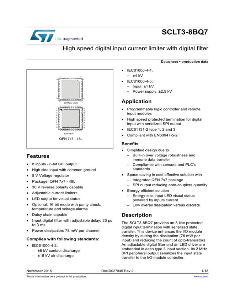
4)1[/
Benefits
• Simplified design due to
– Built-in over voltage robustness and
immune data transfer
– Compliance with sensors and PLC's
standards
Features
• 8 inputs - 8-bit SPI output
• High side input with common ground
• Space saving in cost effective solution with
– Integrated QFN 7x7 package
– SPI output reducing opto-couplers quantity
• 5 V Voltage regulator
• Package: QFN 7x7 - 48L
• 30 V reverse polarity capable
• Energy efficient solution
– Energy-less input LED visual status
powered by inputs current
– Low overall dissipation versus discrete
• Adjustable current limiters
• LED output for visual status
• Optional: 16-bit mode with parity check,
temperature and voltage alarms
• Daisy chain capable
Description
• Input digital filter with adjustable delay: 20 µs
to 3 ms
• Power dissipation: 78 mW per channel
Complies with following standards:
• IEC61000-4-2:
– ±8 kV contact discharge
– ±15 kV air discharge
November 2015
This is information on a product in full production.
The SCLT3-8BQ7 provides an 8-line protected
digital input termination with serialized state
transfer. This device enhances the I/O module
density by cutting the dissipation (78 mW per
input) and reducing the count of opto-transistors.
An adjustable digital filter and an LED driver are
embedded in each type 3 input section. Its 2 MHz
SPI peripheral output serializes the input state
transfer to the I/O module controller.
DocID027845 Rev 2
1/18
www.st.com
Circuit block diagram
1
SCLT3-8BQ7
Circuit block diagram
Figure 1. circuit block diagram
9''
3URWHFWHGLQSXW
9,1 9 5
VPVGLJLWDOILOWHUV
OLQHV
OLQHV
OLQHV
026,
OLQHV
630
ELW
9&
&ORFNGLYLGHU
3RZHU
VXSSO\
3RZHU
UHVHW
9''
9&6
8QGHUYROWDJH
DODUP
2YHUWHPSHUDWXUH
DODUP
&6
6+,)7
&XUUHQW
UHIHUHQFH
2VFLOODWRU
026,
6&.
'95
26&
Figure 2. Basic application schematic
/('
/('
/('
/('
9''
/('
55()
5()
&206
026,
0,62
&6
6&.
0,62
$&3/ :/
$&3/ ./
9''
/('
'95
/('
5 26& 26&
/('
630
&203
9,
9,
DocID027845 Rev 2
9,
9,
9,
5,
,1
,1 5,
,1
,1
9,
5,
5,
,1
9,
,1 5,
5,
5,
,1
9&&
,1 5,
56
5& 9&
9&6
53'
&203
&20 3
2/18
&206
:5,7(
6+,)7
&RQWUROVWDWHUHJLVWHU
5()
0,62
9''
&$3785(
3DULW\
ELWVJHQ
, W R
3URWHFWHGLQSXW
&203
/',
OLQHV
'DWDVWDWHUHJLVWHU
,QSXWVWDWHUHJLVWHU
/'
,1,
9''
0,62
95
7UDQVIHU
ORJLF
,1
9,
SCLT3-8BQ7
1.1
Circuit block diagram
I/O pin description
Table 1. I/O pin descriptions
Name
Type
INI
Power input
LDI
Power output
VC
Power input
24 V sensor power supply
13
VCS
Signal input
24 V sensor power supply sensing input
14
COMP
Ground
VDD
Description
Pin #
Logic input with current limitation, I = 1 to 8
16, 17, 18, 19,
21, 22, 23, 24
LED output driver with current regulation, I =
1 to 8
34, 35, 36, 37,
38, 39, 40, 41
Power ground of power sensor supply
Power output 5 V logic power supply
7, 15, 20, 31
1
COMS
Ground
Signal ground of logic / output section
43
REF
Signal input
Input current limiter reference setting
42
SPM
Signal input
SPI shift register length selector
-SPM to GND --> 16 bits
-SPM to VDD --> 8 bits
4
/CS
Logic input
SPI chip Select signal
48
SCK
Logic input
SPI serial clock signal
47
MOSI
Logic input
SPI serial data input signal
46
DVR
Logic input
Divider ratio selector of the digital input filters
(8 or 64 steps)
2
OSC
Signal input
Delay setting of the digital input filters
3
MISO
Logic output
SPI serial data output signal
44
/MISO
Logic output
Inverting SPI serial data output signal
45
TAB
Substrate
NC
Exposed pad: connected to die substrate, to
be connected to COMP
TAB
Not connected (or to be connected to COMP)
5, 6, 8, 9, 10, 11, 12, 25, 26,
27, 28, 29, 30, 32, 33
DocID027845 Rev 2
3/18
18
Circuit block diagram
SCLT3-8BQ7
/('
/('
/('
/('
/('
5()
&206
0,62
0,62
026,
&6
6&.
Figure 3. Pinout description of the QFN7x7-48L version (top view)
9''
/('
'95
/('
26&
/('
630
1&
1&
1&
1&
&203
&20 3
1&
1&
1&
1&
1&
1&
1&
7$%
1&
1&
1&
,1
,1
,1
,1
&20 3
,1
,1
,1
,1
&20 3
9&6
9&
1&
The package is the QFN7x7-48L exposed pad that improves ground cooling transfer of input
dissipation to the printed board.
Figure 4. Basic module input characteristics in type 3
30
2.1mA
VI (V)
RI = 2.2 kΩ
VI = V IN + RI x IIN
25
2.6mA
ON
RI
20
SCLT
15
11V
10
OFF
5
0
0
4/18
0.5
1
1.5
IIN (mA)
DocID027845 Rev 2
2
2.5
3
SCLT3-8BQ7
2
Characteristic information
Characteristic information
Table 2. Absolute maximum ratings
Symbol
Pin
VCC
Vc
VC
Conditions
Value
Unit
Bus power supply DC voltage
500 Ω < Rc < 2.2 kΩ
-0.3 to 35
V
Vc
SCLT3-8BQ7 power supply voltage
Rc = 0 kΩ
-0.3 to 30
V
ICC
Vc
Maximum bus power supply current
15
mA
VCS
VCS
Sensing bus power supply voltage
-0.3 to 6
V
IDD
VDD
Maximum output power supply current
Rc = 500 Ω
12
mA
VI
INI
Input steady state voltage, I = 1 to 8
RI = 2.2 kΩ
-30 to 35
V
IIN
INI
Input forward current range
-20 to 10
mA
IOSC
OSC
Maximum sourced oscillator current
120
µA
LVI
SCK
/CS
MOSI
Logic input voltage
-0.3 to 6
V
Storage temperature range
-40 to 150
°C
Ambient temperature range
-40 to 105
°C
Tstg
Tamb
All
Parameter name
DocID027845 Rev 2
5/18
18
Characteristic information
SCLT3-8BQ7
Table 3. Operating conditions
Symbol
Pin
VCC
Vc
VDD
VDD
Internal logic power supply voltage
IDD
VDD
Internal logic power supply voltage
Rc > 500 Ω
VI
IN
Input repetitive steady state voltage
RI = 2.2 kΩ(2)
VLD
LDI
Maximum LED output voltage, I = 1 to 8
FIN MAX
IN
Maximum single input frequency
FSCK MAX
ROSC
LV
Tamb
Parameter name
Conditions
Bus power supply steady state voltage
Value
Unit
15 to 35(1)
V
5
V
10
mA
-30 to 35
V
2.7
V
20
kHz
0.1 to 2
MHz
15 k to 1.5 M
Ω
0 to 5.5
V
VCC ≤30 V
-40 to 85
°C
VCC ≤ 24 V
Rth(j-a) = 70 °C/W
-40 to 105
°C
-40 to 150
°C
Rc > 500 Ω
8-bit mode
Maximum SPI clock frequency
OSC
Filter oscillator resistance range
SCK
/CS
MOSI Logic input/output voltages
MISO
/MISO
ALL
Tj
Operating ambient temperature range
Operating junction temperature range
1. 32 V in DC; 35V during 0.5 s max
2. VI = VIN + RI x IIN
Table 4. DC electrical characteristics based on figure 2 application environment
Symbol
Pin
Name
Conditions
Min.
Typ.
Max.
Unit
2.1
2.35
2.6
mA
Input Current limitation
ILIM
IN
Input limiting current
VIN = 5.5 to 26 V
RI = 2.2 kΩ
ION
LDI
On state LED current
VI = 11 V
2
mA
Input digital filter
TOSC
OSC
Oscillator period
ROSC
OSC
Oscillator resistance
CKF period
tCKF
tFT
6/18
IN
ROSC = 51 kΩ
ROSC = 1200 kΩ
1.13
1.37
µs
20
28
µs
51
1200
kΩ
DVR = VDD
64 x TOSC
DVR = COMs
8 x TOSC
Filtering time
2 x tCKF
DocID027845 Rev 2
3 x tCKF
SCLT3-8BQ7
Characteristic information
Table 5. SPI electrical characteristics (Tj = 25 °C, VCC = 24 V, VDD = 5 V respect to COM ground pin;
unless otherwise specified)
Symbol
Pin
Name
Conditions
Min.
Typ.
Max.
Unit
2
MHz
FCK
SCK
Clock frequency
TS
MOSI
Data setup time
MOSI toggling to SCK
rising
TD
MISO
Write out propagation time
SCK falling to MISO
toggling, COUT = 10 pF
TLD
SCK
Enable lead time
/CS falling to SCK
rising
80
ns
THC
SCK
Clock hold time
SCK falling to /CS
rising
160
ns
TDT
/CS
Transfer delay time
/CS rising to /CS falling
TH
MOSI
Data hold time
SCK rising to MOSI
toggling
TDIS
MISO
Data output disable time
/CS rising to MISO
disabled
200
ns
LVIH
MOSI
SCK
/CS
Logic input high voltage
Share of VDD
70
%
Logic input low voltage
Share of VDD
30
Logic output high voltage
IOH = 3mA
4
Logic output low voltage
IOL = 3mA
LVIL
LVOH
/MISO
MISO
LVOL
25
ns
50
150
25
ns
ns
ns
%
4.75
0.25
TRO, TFO
MISO
/MISO
MISO signal fall/rise time
IMISO = 3mA
20
TA
MISO
Output access time
/CS falling to MISO
toggling
40
DuCy
SCK
Clock duty cycle
25
V
1
V
ns
80
ns
75
%
Figure 5. Time diagram
7)5$0(
&6
7&+
7/'
6&.
7&/
06% 0
06% 6
7'7
/6% 0
06% 6
/6% 6
06% 0
7'
7$
0,62
7+&
75
76
7+
026,
7)
7',6
DocID027845 Rev 2
7/18
18
Characteristic information
SCLT3-8BQ7
Table 6. Electromagnetic compatibility ratings
Symbol
Pin
VPPB
VI
VPP
Parameter name(1)
Value
Unit
Peak pulse voltage burst, IEC61000-4-4(2)
4
KV
VI
Peak pulse voltage surge, IEC61000-4-5
1
kV
VPP
VCC
Peak pulse voltage surge, IEC61000-4-5
2.5
kV
VESD
VIN
ESD protection, IEC 61000-4-2, per input
– air
– contact
15
8
kV
1. Test set-up, see application Figure 2.
2. See AN3031.
8/18
DocID027845 Rev 2
SCLT3-8BQ7
Functional description
3
Functional description
3.1
Operation of the SCLT3-8BQ7 with the SPI bus (CPOL = 0,
CPHA = 0)
The SPI bus master controller manages the data transfer with the chip select signal /CS and
controls the data shift in the register with the clock SCK signal.
Figure 6. Serial data format frame
&6
6&.
026,
0,62
'$7$&$3785(
06%0
06%6
/6%0
06%6
/6%6
06%0
The transfer of the SCLT3-8BQ7 input states in the SPI registers starts when the Chip
Select /CS signal falls and ends when this /CS is rising back.
The transfer of data out of the SCLT3-8BQ7 slave MISO output starts immediately when the
chip select /CS goes low.
Then, the input MOSI is captured and presented to the shift register on each rising edge of
the clock SCK. And the data are shifted in this register on each falling edge of the serial
clock SCK, the data bits being written on the output MISO with the most significant bit first.
3.1.1
The serial data Input MOSI
This input signal MOSI is used to shift external data bits into the SCLT3-8BQ7 register from
the most significant MSB bit to the lower significant one LSB. The data bits are captured by
the SCLT3-8BQ7 on the rising edge of the serial clock signal SCK.
3.2
The input digital filter
Depending on the biasing of the SPM pin, the data frame is 8-bits or 16-bits.
A digital filter is implemented between the input state comparator and the input state
register. It consists of a 2-step sampling circuit that is controlled by an oscillator as shown on
Figure 7.
The filtering time tFT is set by the external oscillator resistor and is a function of the oscillator
period tCKF:
•
2 x tCKF < tFT < 3 x tCKF
•
tCKF = Divider ratio x tOSC (ROSC)
DocID027845 Rev 2
9/18
18
Functional description
SCLT3-8BQ7
This period can be adjusted between 20 µs and 3000 µs as shown on Table 7.
Table 7. Typical setting of the digital filter timings
Input speed
Fast
Medium
Slow
Input frequency (kHz)
60
20
5
0.3
Min. filter time tFT (µs)
20
50
230
3000
OSC resistance (kΩ)
51
150
82
1300
CKF period tCKF (µs)
10
25
115
1500
COMS
COM S
VDD
VDD
8
8
64
64
DVR connection
Divider ratio
Being placed in the front end of the module, this filter increases the transient immunity of the
SCLT and its SPI logic circuitry. It also simplifies the input management software task of the
ASIC controller.
Figure 7. Two step digital filter placed after the analog section of the logic input
,1
'
4
'
4
'
4
6
4
&.
4
&.
4
&.
4
287
5
&.)
&.)
,1
287
7
3.3
The SPI data transfer operation
3.3.1
The SPI data frame
Depending on the biasing of the SPM pin, the data frame is 8-bits or 16-bits. The selected
structure of the SPI is a 16-bit word in order to be able to implement the input state data and
some control bits such as the UVA alarm, the 4 checksum bits and the two low & high state
stop bits.
10/18
DocID027845 Rev 2
SCLT3-8BQ7
3.3.2
Functional description
The SPI data transfer
The SCLT3-8BQ7 transfers its 16 data bits through the SPI within one chip select Hi-Lo-Hi
sequence. So, this length defines the minimum length that the shift register of the SPI
master controller is able to capture: 16 bits.
The Table 8 shows the 16-bit mode way the data are transferred starting from the data bits,
the control bits and ending by a stop bit.
Table 8. SPI data transfer organization versus CLT input states with SPM = 0
Bit #
LSB
Bit 1
Bit 2
Bit 3
Bit 4
Bit 5
Bit 6
Bit 7
Control
High
Low
PC4
PC3
PC2
PC1
/OTA
/UVA
Last out
Bit #
Bit 8
Bit 9
Bit 10
Bit 11
Bit 12
Bit 13
Bit 14
MSB
Data
IN 1
IN 2
IN 3
IN 4
IN 5
IN 6
IN 7
IN 8
First out
3.4
Control bit signals of the SPI transferred data frame
3.4.1
The power bus voltage monitoring
The UVA circuit generates the alarm /UVA that is active low when the power bus voltage is
lower than the activation threshold VCON, 17 V typical, and it is disabled high when the
power bus voltage rises above the threshold VCOFF, 18 V typical.
3.4.2
The over temperature alarm
The alarm signal /OTA is enabled, low state active, when the junction temperature is higher
than the activation threshold TON, 150 ºC typical, and it is disabled when the junction
temperature falls below the threshold TOFF, 140ºC typical.
DocID027845 Rev 2
11/18
18
Functional description
3.4.3
SCLT3-8BQ7
The parity checksum bits calculation and transfer
The aim of the parity checksum bit is to detect one error in the transferred SPI word. Several
parity checksum bits are generated and transmitted through the SPI on the control bit #2 to
#5.
In order to calculate parity bit, “exclusive NOR” operations are performed as follow:
Table 9. SCLT3-8BQ7 parity bit calculation example
3.5
IN8
IN7
IN6
IN5
IN4
IN3
IN2
IN1
1
0
0
1
1
0
0
1
PC1
PC2
PC3
PC4
1
1
1
1
Loss of VCC power supply
The operation of the SCLT3-8BQ7 is extended below the levels required in the IEC 61131-2
standard to allow the implementation of the under voltage alarm UVA as described the SPI
control bit section.
If there is no more power feeding on the VCC input, the SCLT3-8BQ7 chip goes to sleep
mode, and the MISO output is forced in low state during SPI transfer attempt. The last SPI
control data bit is a stop bit placed normally in high state all time: the loss of power supply is
detected by checking its state: if low, the output is disabled by the internal power reset POR.
This POR signal is active in low state when VC is less than 9V or the internal power supply
VDD is less than 3.25 V.
Table 10. Logic state of the SPI output versus the power loss signal POR and the SPI
chip select /CS
12/18
POR
/CS
MISO
/MISO
SPI status
1
1
Z
Z
Normal with no communication
1
0
1
0
Normal with communication
1
0
0
1
Normal with communication
0
1
Z
Z
Power loss with no communication
0
0
0
1
Power loss with communication attempt
DocID027845 Rev 2
SCLT3-8BQ7
Functional description
Figure 8. Logic status of the SCLT3-8BQ7 power supply
3RZHUVXSSO \VWDWXV
3RZHUVXSSO\VWDWXV
/RVVRISR ZHU
/RVVRISRZHU
89$ODUP
9
3RZHUJRRG
9
9
9& 9 && 5 & [, & ,''
a9
9
9
9&&
,(&OH YHO
9
9&
89$
&6 /R
325
&6 /R
0,62
&6 /R , 1 $6,& 0,62QRQLQYHU WLQJLVRODWRU
Figure 9. Typical limiting current ILIM versus reference resistance RREF
,/,0 P$
9&& 99 , 9
55() N:
Figure 10. Typical limiting current ILIM versus junction temperature TJ
,/,0 P$
5UHI NȍZLWK5,1 Nȍ9, WR99 && WR9
7- &
DocID027845 Rev 2
13/18
18
Functional description
SCLT3-8BQ7
Figure 11. Relative variation of minimum filter time tFT versus junction temperature TJ
7)70,1 7 )70,1 &
526& N
526& 0
7- &
Figure 12. Variation of junction to ambient thermal resistance Rth(j-a) versus printed
circuit board copper surface SCU
5WKMD&:
3ULQWHGFLUFXLWERDUG )5HSR[\
VLQJOHOD\HU FRSSHUWKLFNQHVV P
6 &8PPð 14/18
DocID027845 Rev 2
SCLT3-8BQ7
4
Package information
Package information
In order to meet environmental requirements, ST offers these devices in different grades of
ECOPACK® packages, depending on their level of environmental compliance. ECOPACK®
specifications, grade definitions and product status are available at: www.st.com.
ECOPACK® is an ST trademark.
QFN7x7-48L package information
Figure 13. QFN7x7-48L package outline
&
'
H
3,1
$
H
E
(
(
/
E
.
'
$
$
'
4.1
GGG &
#PUUPNWJFX
5PQWJFX
DocID027845 Rev 2
15/18
18
Package information
SCLT3-8BQ7
Table 11. QFN7x7-48L package mechanical data
Dimensions
Ref.
Inches(1)
Millimeters
Min.
Typ.
Max.
Min.
Typ.
Max.
0.80
0.90
1.00
0.0315
0.0354
0.0394
A1
0.02
0.05
0.0008
0.0020
A3
0.203
A
b
0.18
0.25
0.008
0.30
0.0071
D
7.00
0.275
E
7.00
0.275
e
0.50
0.019
0.0118
D2
5.00
5.15
5.25
0.197
0.203
0.206
E2
5.00
5.15
5.25
0.197
0.203
0.206
K
0.20
L
0.30
0.015
0.019
0.008
0.40
0.50
0.011
1. Values in inches are converted from mm and rounded to 4 decimal digits.
16/18
0.0100
DocID027845 Rev 2
SCLT3-8BQ7
5
Ordering information
Ordering information
Figure 14. Ordering information scheme
6& /7
±
%
4 6HULDOFXUUHQWOLPLWHUWHUPLQDWLRQ
P$FXUUHQWVHWWLQJ
HLJKWFKDQQHOV
%(0&OHYHO
N9DFFRUGLQJ WR,(&
44)1 /[
Table 12. Ordering information
6
Order code
Marking
Package
Weight
Base qty
Delivery mode
SCLT3-8BQ7-TR
SCLT3-8BQ7
QFN7x7-48L
114 mg
2500
Tape and reel
Revision history
Table 13. Document revision history
Date
Revision
Changes
29-July-2015
1
Initial release.
12-Nov-2015
2
Updated Table 4.
DocID027845 Rev 2
17/18
18
SCLT3-8BQ7
IMPORTANT NOTICE – PLEASE READ CAREFULLY
STMicroelectronics NV and its subsidiaries (“ST”) reserve the right to make changes, corrections, enhancements, modifications, and
improvements to ST products and/or to this document at any time without notice. Purchasers should obtain the latest relevant information on
ST products before placing orders. ST products are sold pursuant to ST’s terms and conditions of sale in place at the time of order
acknowledgement.
Purchasers are solely responsible for the choice, selection, and use of ST products and ST assumes no liability for application assistance or
the design of Purchasers’ products.
No license, express or implied, to any intellectual property right is granted by ST herein.
Resale of ST products with provisions different from the information set forth herein shall void any warranty granted by ST for such product.
ST and the ST logo are trademarks of ST. All other product or service names are the property of their respective owners.
Information in this document supersedes and replaces information previously supplied in any prior versions of this document.
© 2015 STMicroelectronics – All rights reserved
18/18
DocID027845 Rev 2
