TS19751 Single-Stage Buck Current Control LED Driver with High
advertisement

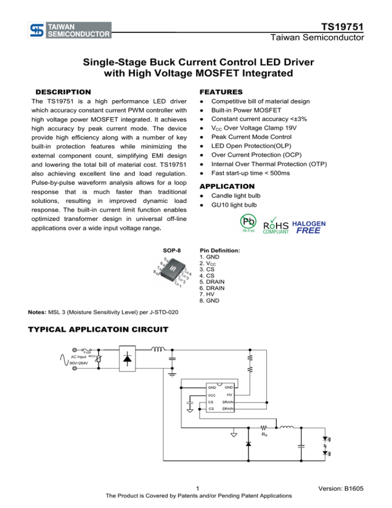
TS19751 Taiwan Semiconductor Single-Stage Buck Current Control LED Driver with High Voltage MOSFET Integrated DESCRIPTION FEATURES The TS19751 is a high performance LED driver ● Competitive bill of material design which accuracy constant current PWM controller with high accuracy by peak current mode. The device ● ● ● Built-in Power MOSFET Constant current accuracy <±3% VCC Over Voltage Clamp 19V provide high efficiency along with a number of key ● Peak Current Mode Control built-in protection features while minimizing the ● LED Open Protection(OLP) external component count, simplifying EMI design ● Over Current Protection (OCP) and lowering the total bill of material cost. TS19751 ● Internal Over Thermal Protection (OTP) also achieving excellent line and load regulation. ● Fast start-up time < 500ms Pulse-by-pulse waveform analysis allows for a loop APPLICATION high voltage power MOSFET integrated. It achieves response that is much faster than traditional solutions, resulting in improved dynamic load response. The built-in current limit function enables ● Candle light bulb ● GU10 light bulb optimized transformer design in universal off-line applications over a wide input voltage range. SOP-8 Pin Definition: 1. GND 2. VCC 3. CS 4. CS 5. DRAIN 6. DRAIN 7. HV 8. GND Notes: MSL 3 (Moisture Sensitivity Level) per J-STD-020 TYPICAL APPLICATOIN CIRCUIT 1 The Product is Covered by Patents and/or Pending Patent Applications Version: B1605 TS19751 Taiwan Semiconductor ABSOLUTE MAXIMUM RATINGS (TA = 25°C unless otherwise specified) (Note 1) PARAMETER SYMBOL LIMIT UNIT Power Supply Pin VCC 40 V CS Voltage to GND VCS -0.3 to 5.5 V HV Voltage to GND VHV -0.3 to 500 V Operating Temperature Range TOPR -40 to +105 °C Junction Temperature Range TJ -40 to +150 °C Storage Temperature Range TSTG -65 to +150 °C Lead Temperature (Soldering 10 sec) TLEAD 260 °C PD 0.6 W HBM 2 kV MM 200 V SYMBOL LIMIT UNIT RӨJC 50 o 208 o Power Dissipation @ TA=25 °C ESD Rating (Human Body Mode) ESD Rating (Machine Mode) (Note 2) (Note 2) THERMAL PERFORMANCE (Note 3) PARAMETER Thermal Resistance - Junction to Case Thermal Resistance - Junction to Ambient RӨJA C/W C/W RECOMMENDED OPERATING CONDITION (TA = 25°C unless otherwise specified) (Note 4) PARAMETER SYMBOL LIMIT UNIT Power Supply Pin VCC 19 V CS Voltage to GND VCS -0.3 to 5 V HV Voltage to GND VHV -0.3 to 500 V Operating Junction Temperature Range TJ -40 to +150 °C Operating Ambient Temperature Range TOPA -40 to +85 °C ELECTRICAL SPECIFICATIONS (TA = 25°C unless otherwise specified) PARAMETER SYMBOL CONDITION MIN TYP MAX UNIT VCC= VUVLO(on) -1V -- 45 -- μA With 1nF load on out pin -- 2 -- mA Supply Voltage Start-up Current VCC(ST) Operating Current IOPA UVLO(off) VUVLO(off) 7 8 9 V UVLO(on) VUVLO(on) 16 17.5 19 V VVCC 17 19 21 V VFB 0.194 0.2 0.206 V CS Limit Voltage VOCP -- 0.5 -- V Leading-Edge Blanking Time LEBt -- 400 -- ns -- 100 -- ns 3 4.5 6 kHz VCC Clamp Voltage Voltage Feedback Feedback Reference Voltage Current Sensing Delay to Output Switching Frequency Start Frequency fSTR 2 The Product is Covered by Patents and/or Pending Patent Applications Version: B1605 TS19751 Taiwan Semiconductor ELECTRICAL SPECIFICATIONS (TA = 25°C unless otherwise specified) PARAMETER SYMBOL CONDITION MIN TYP MAX UNIT TS19751ACS 500 -- -- V TS19751BCS 650 -- -- V TS19751ACS -- -- 30 Ω TS19751BCS -- -- 17 Ω Thermal Shutdown -- 150 -- °C Thermal Shutdown Release -- 120 -- °C MOSFET Section Drain-Source Breakdown BVDS Voltage Drain-Source On-Resistance Thermal Section RDS(ON) (Note 5, 6) Note: 1. Stresses listed as the above “Absolute Maximum Ratings” may cause permanent damage to the device. These are for stress ratings. Functional operation of the device at these or any other conditions beyond those indicated in the operational sections of the specifications is not implied. Exposure to absolute maximum rating conditions for extended periods may remain possibility to affect device reliability. 2. Devices are ESD sensitive. Handing precaution recommended. 3. Thermal Resistance is specified with the component mounted on a low effective thermal conductivity test board in free air at TA=25°C. 4. The device is not guaranteed to function outside its operating conditions. 5. Guaranteed by design. 6. Auto Recovery Type. ORDERING INFORMATION PART NO. PACKAGE PACKING TS19751ACS RLG SOP-8 2,500pcs / 13”Reel TS19751BCS RLG SOP-8 2,500pcs / 13”Reel 3 The Product is Covered by Patents and/or Pending Patent Applications Version: B1605 TS19751 Taiwan Semiconductor FUNCTION BLOCK PIN DESCRIPTION PIN NO. NAME FUNCTION 1,8 GND Ground return for all internal circuitry. 2 VCC Power supply pin for all internal circuitry. 3,4 CS Input current sense pin. 5,6 DRAIN 7 HV Drain of internal HV MOS. HV start up pin 4 The Product is Covered by Patents and/or Pending Patent Applications Version: B1605 TS19751 Taiwan Semiconductor APPLICATION INFORMATION Start-up Current The typical start-up current is around 45μA. The TS19751 has a built-in HV start-up circuit that avoids the need for a start-up resistor. Under Voltage Lockout (UVLO) A hysteresis UVLO comparator is implemented in TS19751. The turn-on and turn-off thresholds level are fixed at 17.5V and 8V respectively. This hysteresis shown in Fig.1 ensures that the start-up capacitor will be adequate to supply the chip during start-up. For quick start-up of the LED driver, the start-up resistor should be matched with the start-up capacitor. Fig.1 Leading-Edge Blanking (LEB) Each time the power MOSFET is switched on, a turn-on spike will inevitably occur at the sense resistor. To avoid fault trigger, a 400ns leading-edge blanking time is built in. Conventional RC filtering can therefore be omitted. During this blanking period, the current-limit comparator is disabled and cannot switch off the gate driver. VCC Over Voltage Clamp VCC is clamped to 19V by an internal clamping circuit to guarantee IC normal operation. Over Current Protection (OCP) The TS19751 has built-in cycle by cycle over current protection function on CS pin. As the CS pin voltage is larger than VOCP (0.5V), the gate output will be turned off immediately to avoid the driver board to be burned out. Open load Protection (OLP) To prevent the LED driver from being damaged, the TS19751 has an implemented OLP function. The open load protection will shut the gate driver when minimum off time keep shorter than 4.5uS. Over Temperature Protection (OTP) Internal 165℃ comparator will trigger temperature protection (OTP). OTP will shut down system, until internal temperature back to 120℃. 5 The Product is Covered by Patents and/or Pending Patent Applications Version: B1605 TS19751 Taiwan Semiconductor PACKAGE OUTLINE DIMENSIONS (Unit: Millimeters) SOP-8 SUGGESTED PAD LAYOUT (Unit: Millimeters) MARKING DIAGRAM x = Device code A/B Y = Year Code M = Month Code for Halogen Free Product O =Jan P =Feb Q =Mar R =Apr S =May T =Jun U =Jul V =Aug W =Sep X =Oct Y =Nov Z =Dec L = Lot Code (1~9, A~Z) 6 The Product is Covered by Patents and/or Pending Patent Applications Version: B1605 TS19751 Taiwan Semiconductor Notice Specifications of the products displayed herein are subject to change without notice. TSC or anyone on its behalf, assumes no responsibility or liability for any errors or inaccuracies. Information contained herein is intended to provide a product description only. No license, express or implied, to any intellectual property rights is granted by this document. Except as provided in TSC’s terms and conditions of sale for such products, TSC assumes no liability whatsoever, and disclaims any express or implied warranty, relating to sale and/or use of TSC products including liability or warranties relating to fitness for a particular purpose, merchantability, or infringement of any patent, copyright, or other intellectual property right. The products shown herein are not designed for use in medical, life-saving, or life-sustaining applications. Customers using or selling these products for use in such applications do so at their own risk and agree to fully indemnify TSC for any damages resulting from such improper use or sale. 7 The Product is Covered by Patents and/or Pending Patent Applications Version: B1605


